- 您現(xiàn)在的位置:買賣IC網(wǎng) > PDF目錄93260 > DS1249AB-70 (DALLAS SEMICONDUCTOR) 256K X 8 NON-VOLATILE SRAM MODULE, 70 ns, DIP32 PDF資料下載
參數(shù)資料
| 型號: | DS1249AB-70 |
| 廠商: | DALLAS SEMICONDUCTOR |
| 元件分類: | Static RAM |
| 英文描述: | 256K X 8 NON-VOLATILE SRAM MODULE, 70 ns, DIP32 |
| 封裝: | 0.740 INCH, EXTENDED MODULE, DIP-32 |
| 文件頁數(shù): | 7/8頁 |
| 文件大?。?/td> | 140K |
| 代理商: | DS1249AB-70 |
DS1249Y/AB
7 of 8
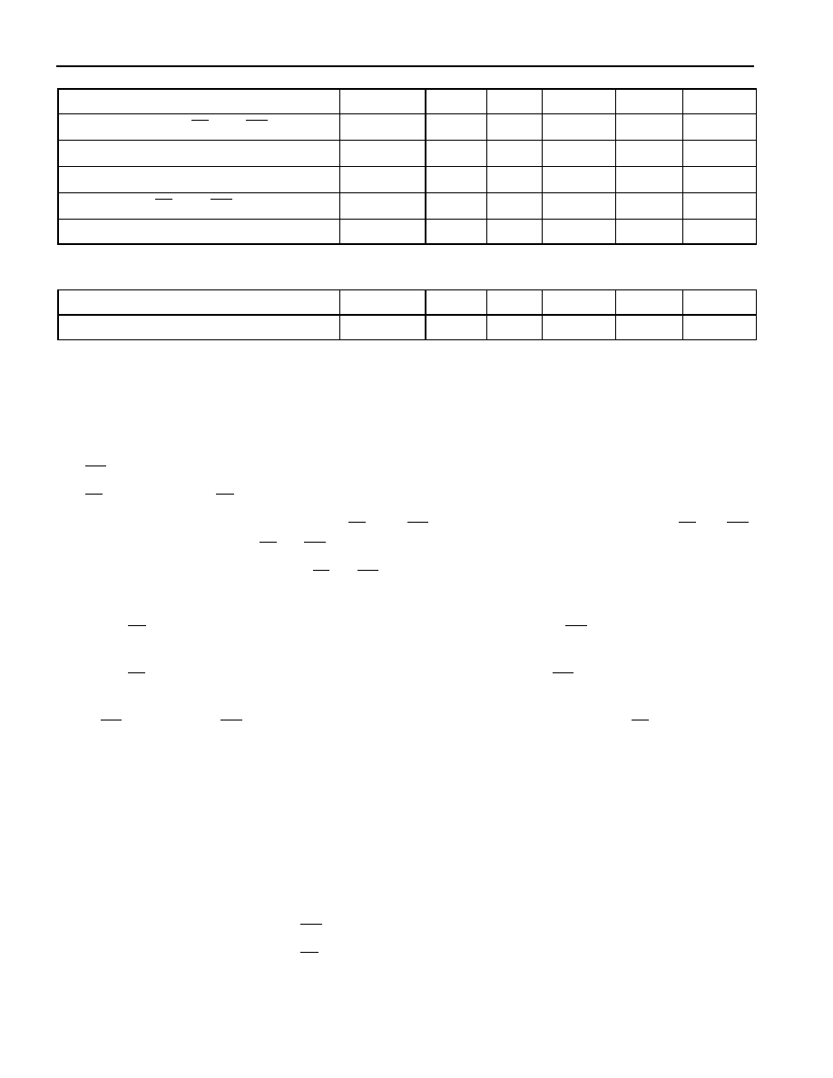
POWER-DOWN/POWER-UP TIMING
(tA: See Note 10)
PARAMETER
SYMBOL
MIN
TYP
MAX
UNITS
NOTES
VCC Fail Detect to CE and WE Inactive
tPD
1.5
s
11
VCC slew from VTP to 0V
tF
150
s
VCC slew from 0V to VTP
tR
150
s
VCC Valid to CE and WE Inactive
tPU
2ms
VCC Valid to End of Write Protection
tREC
125
ms
(tA=25
°C)
PARAMETER
SYMBOL
MIN
TYP
MAX
UNITS
NOTES
Expected Data Retention Time
tDR
10
years
9
WARNING:
Under no circumstance are negative undershoots, of any amplitude, allowed when device is in battery
backup mode.
NOTES:
1.
WE
is high for a Read Cycle.
2. OE = VIH or VIL. If OE = VIH during write cycle, the output buffers remain in a high impedance state.
3. tWP is specified as the logical AND of CE and WE . tWP is measured from the latter of CE or WE
going low to the earlier of CE or WE going high.
4. tDS is measured from the earlier of CE or WE going high.
5. These parameters are sampled with a 5 pF load and are not 100% tested.
6. If the CE low transition occurs simultaneously with or latter than the WE low transition in Write
Cycle 1, the output buffers remain in a high-impedance state during this period.
7. If the CE high transition occurs prior to or simultaneously with the WE high transition, the output
buffers remain in high-impedance state during this period.
8. If WE is low or the WE low transition occurs prior to or simultaneously with the CE low transition,
the output buffers remain in a high-impedance state during this period.
9. Each DS1249 has a built-in switch that disconnects the lithium source until VCC is first applied by the
user. The expected tDR is defined as accumulative time in the absence of VCC starting from the time
power is first applied by the user.
10. All AC and DC electrical characteristics are valid over the full operating temperature range. For
commercial products, this range is 0
°C to 70°C. For industrial products (IND), this range is -40°C to
+85
°C.
11. In a power-down condition the voltage on any pin may not exceed the voltage on VCC.
12. tWR1 and tDH1 are measured from WE going high.
13. tWR2 and tDH2 are measured from CE going high.
相關(guān)PDF資料 |
PDF描述 |
|---|---|
| DS1249AB-100 | 256K X 8 NON-VOLATILE SRAM MODULE, 100 ns, DIP32 |
| DS1249AB | 256K X 8 NON-VOLATILE SRAM MODULE, 70 ns, PDIP32 |
| DS1249Y | 256K X 8 NON-VOLATILE SRAM MODULE, 70 ns, PDIP32 |
| DS1249Y-70 | 256K X 8 NON-VOLATILE SRAM MODULE, 70 ns, DMA32 |
| DS1249Y-100 | 256K X 8 NON-VOLATILE SRAM MODULE, 100 ns, DMA32 |
相關(guān)代理商/技術(shù)參數(shù) |
參數(shù)描述 |
|---|---|
| DS1249AB-70# | 功能描述:NVRAM 2048K NV SRAM RoHS:否 制造商:Maxim Integrated 數(shù)據(jù)總線寬度:8 bit 存儲容量:1024 Kbit 組織:128 K x 8 接口類型:Parallel 訪問時間:70 ns 電源電壓-最大:5.5 V 電源電壓-最小:4.5 V 工作電流:85 mA 最大工作溫度:+ 70 C 最小工作溫度:0 C 封裝 / 箱體:EDIP 封裝:Tube |
| DS1249AB-70IND | 功能描述:NVRAM 2048K NV SRAM RoHS:否 制造商:Maxim Integrated 數(shù)據(jù)總線寬度:8 bit 存儲容量:1024 Kbit 組織:128 K x 8 接口類型:Parallel 訪問時間:70 ns 電源電壓-最大:5.5 V 電源電壓-最小:4.5 V 工作電流:85 mA 最大工作溫度:+ 70 C 最小工作溫度:0 C 封裝 / 箱體:EDIP 封裝:Tube |
| DS1249AB-70-IND | 制造商:未知廠家 制造商全稱:未知廠家 功能描述:NVRAM (Battery Based) |
| DS1249AB-70IND# | 功能描述:NVRAM 2048K NV SRAM RoHS:否 制造商:Maxim Integrated 數(shù)據(jù)總線寬度:8 bit 存儲容量:1024 Kbit 組織:128 K x 8 接口類型:Parallel 訪問時間:70 ns 電源電壓-最大:5.5 V 電源電壓-最小:4.5 V 工作電流:85 mA 最大工作溫度:+ 70 C 最小工作溫度:0 C 封裝 / 箱體:EDIP 封裝:Tube |
| DS1249AB-85 | 功能描述:NVRAM 2048K NV SRAM RoHS:否 制造商:Maxim Integrated 數(shù)據(jù)總線寬度:8 bit 存儲容量:1024 Kbit 組織:128 K x 8 接口類型:Parallel 訪問時間:70 ns 電源電壓-最大:5.5 V 電源電壓-最小:4.5 V 工作電流:85 mA 最大工作溫度:+ 70 C 最小工作溫度:0 C 封裝 / 箱體:EDIP 封裝:Tube |
發(fā)布緊急采購,3分鐘左右您將得到回復。