- 您現(xiàn)在的位置:買(mǎi)賣(mài)IC網(wǎng) > PDF目錄376803 > DM93L08 PDF資料下載
參數(shù)資料
| 型號(hào): | DM93L08 |
| 文件頁(yè)數(shù): | 86/158頁(yè) |
| 文件大小: | 2668K |
| 代理商: | DM93L08 |
第1頁(yè)第2頁(yè)第3頁(yè)第4頁(yè)第5頁(yè)第6頁(yè)第7頁(yè)第8頁(yè)第9頁(yè)第10頁(yè)第11頁(yè)第12頁(yè)第13頁(yè)第14頁(yè)第15頁(yè)第16頁(yè)第17頁(yè)第18頁(yè)第19頁(yè)第20頁(yè)第21頁(yè)第22頁(yè)第23頁(yè)第24頁(yè)第25頁(yè)第26頁(yè)第27頁(yè)第28頁(yè)第29頁(yè)第30頁(yè)第31頁(yè)第32頁(yè)第33頁(yè)第34頁(yè)第35頁(yè)第36頁(yè)第37頁(yè)第38頁(yè)第39頁(yè)第40頁(yè)第41頁(yè)第42頁(yè)第43頁(yè)第44頁(yè)第45頁(yè)第46頁(yè)第47頁(yè)第48頁(yè)第49頁(yè)第50頁(yè)第51頁(yè)第52頁(yè)第53頁(yè)第54頁(yè)第55頁(yè)第56頁(yè)第57頁(yè)第58頁(yè)第59頁(yè)第60頁(yè)第61頁(yè)第62頁(yè)第63頁(yè)第64頁(yè)第65頁(yè)第66頁(yè)第67頁(yè)第68頁(yè)第69頁(yè)第70頁(yè)第71頁(yè)第72頁(yè)第73頁(yè)第74頁(yè)第75頁(yè)第76頁(yè)第77頁(yè)第78頁(yè)第79頁(yè)第80頁(yè)第81頁(yè)第82頁(yè)第83頁(yè)第84頁(yè)第85頁(yè)當(dāng)前第86頁(yè)第87頁(yè)第88頁(yè)第89頁(yè)第90頁(yè)第91頁(yè)第92頁(yè)第93頁(yè)第94頁(yè)第95頁(yè)第96頁(yè)第97頁(yè)第98頁(yè)第99頁(yè)第100頁(yè)第101頁(yè)第102頁(yè)第103頁(yè)第104頁(yè)第105頁(yè)第106頁(yè)第107頁(yè)第108頁(yè)第109頁(yè)第110頁(yè)第111頁(yè)第112頁(yè)第113頁(yè)第114頁(yè)第115頁(yè)第116頁(yè)第117頁(yè)第118頁(yè)第119頁(yè)第120頁(yè)第121頁(yè)第122頁(yè)第123頁(yè)第124頁(yè)第125頁(yè)第126頁(yè)第127頁(yè)第128頁(yè)第129頁(yè)第130頁(yè)第131頁(yè)第132頁(yè)第133頁(yè)第134頁(yè)第135頁(yè)第136頁(yè)第137頁(yè)第138頁(yè)第139頁(yè)第140頁(yè)第141頁(yè)第142頁(yè)第143頁(yè)第144頁(yè)第145頁(yè)第146頁(yè)第147頁(yè)第148頁(yè)第149頁(yè)第150頁(yè)第151頁(yè)第152頁(yè)第153頁(yè)第154頁(yè)第155頁(yè)第156頁(yè)第157頁(yè)第158頁(yè)
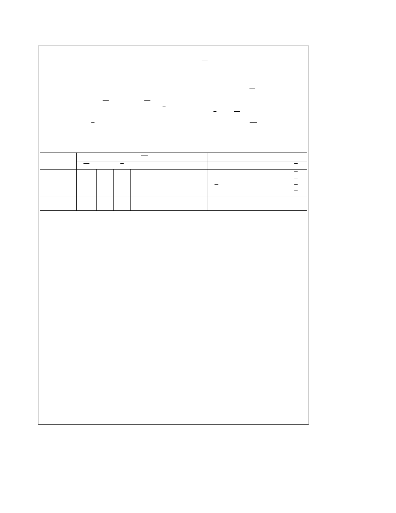
Functional Description
The Logic Diagrams and Truth Table indicate the functional
characteristics of the 93L00 4-bit shift register. The device is
useful in a wide variety of shifting, counting and storage
applications. It performs serial, parallel, serial-to-parallel, or
parallel-to-serial data transfers.
The 93L00 has two primary modes of operation, shift right
(Q0
Q1) and parallel load, which are controlled by the
state of the Parallel Enable (PE) input. When the PE input is
HIGH, serial data enters the first flip-flop Q0 via the J and K
inputs
and
is
one
Q0
Q1
x
Q2
x
Q3
following
clock transition. The JK inputs provide the flexibility of the
JK type input for special applications, and the simple D-type
input for general applications by tying the two pins together.
bit
in
the
LOW-to-HIGH
direction
each
When the PE input is LOW, the 93L00 appears as four com-
mon clocked D flip-flops. The data on the parallel inputs
P0–P3 is transferred to the respective Q0–Q3 outputs fol-
lowing the LOW-to-HIGH clock transition. Shift left opera-
tion (Q3
Q2) can be achieved by tying the Qn outputs to
the Pn
b
1 inputs and holding the PE input LOW.
All serial and parallel data transfers are synchronous, occur-
ing after each LOW-to-HIGH clock transition. Since the
93L00 utilizes edge triggering, there is no restriction on the
activity of the J, K, Pn and PE inputs for logic operationDex-
cept for the setup and release time requirements. A LOW on
the asynchronous Master Reset (MR) input sets all Q out-
puts LOW, independent of any other input condition.
Truth Table
Operating
Mode
Inputs (MR
e
H)
Outputs
@
t
n
a
1
PE
J
K
P0
P1
P2
P3
Q0
Q1
Q2
Q3
Q3
H
H
H
H
L
L
H
H
L
H
L
H
X
X
X
X
X
X
X
X
X
X
X
X
X
X
X
X
L
Q0
Q0
Q0
Q0
Q1
Q1
Q1
Q1
Q2
Q2
Q2
Q2
Q2
Q2
Q2
Q2
Shift Mode
Q0
Q0
H
Parallel
Entry Mode
L
L
X
X
X
X
L
H
L
H
L
H
L
H
L
H
L
H
L
H
L
H
H
L
*
t
n
a
1
e
Indicates state after next LOW-to-HIGH clock transition.
H
e
HIGH Voltage Level
L
e
LOW Voltage Level
X
e
Immaterial
4
相關(guān)PDF資料 |
PDF描述 |
|---|---|
| DM93L09 | |
| DM93L10 | |
| DM93L12 | |
| DM93L16 | |
| DM93L21 | |
相關(guān)代理商/技術(shù)參數(shù) |
參數(shù)描述 |
|---|---|
| DM93L09 | 制造商:未知廠家 制造商全稱(chēng):未知廠家 功能描述: |
| DM93L10 | 制造商:未知廠家 制造商全稱(chēng):未知廠家 功能描述: |
| DM93L12 | 制造商:未知廠家 制造商全稱(chēng):未知廠家 功能描述: |
| DM93L14 | 制造商:FAIRCHILD 制造商全稱(chēng):Fairchild Semiconductor 功能描述:Quad Latch |
| DM93L14N | 功能描述:閉鎖 DISC BY MFG 7/03 RoHS:否 制造商:Micrel 電路數(shù)量:1 邏輯類(lèi)型:CMOS 邏輯系列:TTL 極性:Non-Inverting 輸出線路數(shù)量:9 高電平輸出電流: 低電平輸出電流: 傳播延遲時(shí)間: 電源電壓-最大:12 V 電源電壓-最小:5 V 最大工作溫度:+ 85 C 最小工作溫度:- 40 C 封裝 / 箱體:SOIC-16 封裝:Reel |
發(fā)布緊急采購(gòu),3分鐘左右您將得到回復(fù)。