- 您現(xiàn)在的位置:買賣IC網(wǎng) > PDF目錄378516 > CYP15G0401DXB-BGC (CYPRESS SEMICONDUCTOR CORP) PREMIUM VGA CABLE W/AUDIO5FT, HD15 & 3.5MM M-M PDF資料下載
參數(shù)資料
| 型號(hào): | CYP15G0401DXB-BGC |
| 廠商: | CYPRESS SEMICONDUCTOR CORP |
| 元件分類: | 通信及網(wǎng)絡(luò) |
| 英文描述: | PREMIUM VGA CABLE W/AUDIO5FT, HD15 & 3.5MM M-M |
| 中文描述: | SPECIALTY TELECOM CIRCUIT, PBGA256 |
| 封裝: | BGA-256 |
| 文件頁數(shù): | 2/48頁 |
| 文件大?。?/td> | 1115K |
| 代理商: | CYP15G0401DXB-BGC |
第1頁當(dāng)前第2頁第3頁第4頁第5頁第6頁第7頁第8頁第9頁第10頁第11頁第12頁第13頁第14頁第15頁第16頁第17頁第18頁第19頁第20頁第21頁第22頁第23頁第24頁第25頁第26頁第27頁第28頁第29頁第30頁第31頁第32頁第33頁第34頁第35頁第36頁第37頁第38頁第39頁第40頁第41頁第42頁第43頁第44頁第45頁第46頁第47頁第48頁
CYP15G0401DXA
PRELIMINARY
Document #: 38-02002 Rev. *B
Page 2 of 48
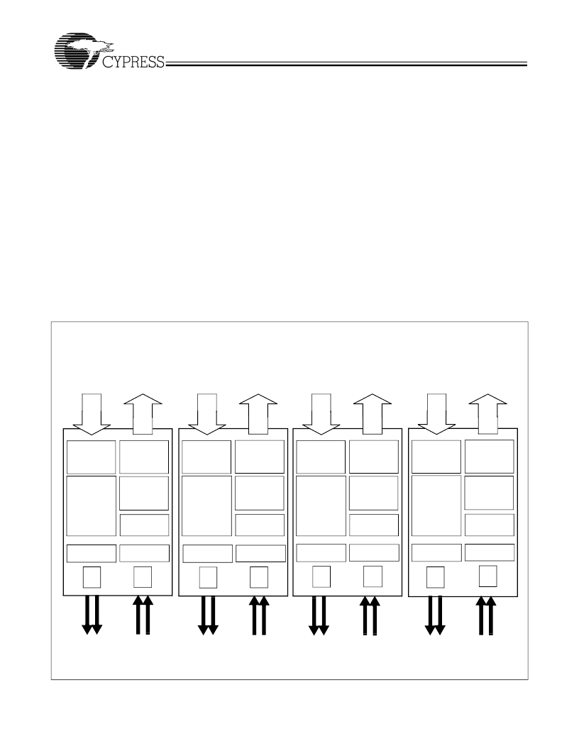
The transmit section of the CYP15G0401DXA Quad HOTLink
II consists of four byte-wide channels that can be operated
independently or bonded to form wider buses. Each channel
can accept either 8-bit data characters or pre-encoded 10-bit
transmission characters. Data characters are passed from the
Transmit Input Register to an embedded 8B/10B Encoder to
improve their serial transmission characteristics. These en-
coded characters are then serialized and output from dual
Positive ECL (PECL) compatible differential transmission-line
drivers at a bit-rate of either 10- or 20-times the input reference
clock.
The receive section of the CYP15G0401DXA Quad HOTLink
II consists of four byte-wide channels that can be operated
independently or synchronously bonded for greater band-
width. Each channel accepts a serial bit-stream from one of
two PECL-compatible differential line receivers and, using a
completely integrated PLL Clock Synchronizer, recovers the
timing information necessary for data reconstruction. Each re-
covered bit-stream is deserialized and framed into characters,
8B/10B decoded, and checked for transmission errors. Recov-
ered decoded characters are then written to an internal Elas-
ticity Buffer, and presented to the destination host system. The
integrated 8B/10B encoder/decoder may be bypassed for sys-
tems that present externally encoded or scrambled data at the
parallel interface.
CYP15G0401DXA Transceiver Logic Block Diagram
For those systems using buses wider than a single byte, the
four independent receive paths can be bonded together to al-
low synchronous delivery of data across a two-byte-wide (16-
bit) path, or across all four bytes (32-bit). Multiple
CYP15G0401DXA devices may be bonded together to provide
synchronous transport of buses wider than 32 bits.
The parallel I/O interface may be configured for numerous
forms of clocking to provide the highest flexibility in system
architecture. In additional to clocking the transmit path inter-
faces from one or multiple sources, the receive interface may
be configured to present data relative to a recovered clock
(output) or to a local reference clock (input).
Each transmit and receive channel contains independent
Built-In Self-Test (BIST) pattern generators and checkers. This
BIST hardware allows at-speed testing of the high-speed se-
rial data paths in each transmit and receive section, and
across the interconnecting links.
HOTLink-II devices are ideal for a variety of applications where
parallel interfaces can be replaced with high-speed, point-to-
point serial links. Some applications include interconnecting
workstations, backplanes, servers, mass storage, and video
transmission equipment.
x10
Serializer
Phase
Align
Buffer
Encoder
8B/10B
Decoder
8B/10B
x11
Framer
Deserializer
TX
RX
x10
Serializer
Encoder
8B/10B
Decoder
8B/10B
x11
Framer
Deserializer
TX
RX
x10
Serializer
Encoder
8B/10B
Decoder
8B/10B
x11
Framer
Deserializer
TX
RX
x10
Serializer
Encoder
8B/10B
Decoder
8B/10B
x11
Framer
Deserializer
TX
RX
T
R
T
R
T
R
T
R
O
A
±
O
±
I
±
I
±
O
±
O
±
I
±
I
±
O
±
O
±
I
±
I
±
O
±
O
±
I
±
I
±
Phase
Align
Buffer
Phase
Align
Buffer
Phase
Align
Buffer
Elasticity
Buffer
Elasticity
Buffer
Elasticity
Buffer
Elasticity
Buffer
T
R
T
R
T
R
T
R
相關(guān)PDF資料 |
PDF描述 |
|---|---|
| CYP15G0401DXB-BGI | Quad HOTLink II Transceiver |
| CYP15G0401DXA-BGC | Quad HOTLink II Transceiver |
| CYP15G0401DXA-BGI | Quad HOTLink II Transceiver |
| CYRF6936 | WirelessUSB LP 2.4GHz Radio SoC(WirelessUSB LP 2.4GHz無線SoC) |
| CYV15G0104TRB | Independent Clock HOTLink II Serializer and Reclocking Deserializer(獨(dú)立時(shí)鐘,HOTLink II并串轉(zhuǎn)換器及時(shí)鐘恢復(fù)串并轉(zhuǎn)換器) |
相關(guān)代理商/技術(shù)參數(shù) |
參數(shù)描述 |
|---|---|
| CYP15G0401DXB-BGI | 功能描述:電信線路管理 IC Dual Channel XCVR 1.5Gbps Bckplane IND RoHS:否 制造商:STMicroelectronics 產(chǎn)品:PHY 接口類型:UART 電源電壓-最大:18 V 電源電壓-最小:8 V 電源電流:30 mA 最大工作溫度:+ 85 C 最小工作溫度:- 40 C 安裝風(fēng)格:SMD/SMT 封裝 / 箱體:VFQFPN-48 封裝:Tray |
| CYP15G0401DXB-BGXC | 功能描述:電信線路管理 IC Dual Channel XCVR 1.5Gbps Bckplane COM RoHS:否 制造商:STMicroelectronics 產(chǎn)品:PHY 接口類型:UART 電源電壓-最大:18 V 電源電壓-最小:8 V 電源電流:30 mA 最大工作溫度:+ 85 C 最小工作溫度:- 40 C 安裝風(fēng)格:SMD/SMT 封裝 / 箱體:VFQFPN-48 封裝:Tray |
| CYP15G0401DXB-BGXCKG | 制造商:Rochester Electronics LLC 功能描述: 制造商:Cypress Semiconductor 功能描述: |
| CYP15G0401DXBBGXI | 制造商:Cypress Semiconductor 功能描述: |
| CYP15G0401DXB-BGXI | 功能描述:電信線路管理 IC Quad HOTLink II XCVR Ch 1.5Gbps Backplane RoHS:否 制造商:STMicroelectronics 產(chǎn)品:PHY 接口類型:UART 電源電壓-最大:18 V 電源電壓-最小:8 V 電源電流:30 mA 最大工作溫度:+ 85 C 最小工作溫度:- 40 C 安裝風(fēng)格:SMD/SMT 封裝 / 箱體:VFQFPN-48 封裝:Tray |
發(fā)布緊急采購(gòu),3分鐘左右您將得到回復(fù)。