- 您現(xiàn)在的位置:買賣IC網(wǎng) > PDF目錄378514 > CY8C21234-24PVX (Cypress Semiconductor Corp.) PSoC Mixed-Signal Array PDF資料下載
參數(shù)資料
| 型號: | CY8C21234-24PVX |
| 廠商: | Cypress Semiconductor Corp. |
| 英文描述: | PSoC Mixed-Signal Array |
| 中文描述: | PSoC混合信號陣列 |
| 文件頁數(shù): | 16/35頁 |
| 文件大?。?/td> | 376K |
| 代理商: | CY8C21234-24PVX |
第1頁第2頁第3頁第4頁第5頁第6頁第7頁第8頁第9頁第10頁第11頁第12頁第13頁第14頁第15頁當前第16頁第17頁第18頁第19頁第20頁第21頁第22頁第23頁第24頁第25頁第26頁第27頁第28頁第29頁第30頁第31頁第32頁第33頁第34頁第35頁
April 20, 2005
Document No. 38-12025 Rev. *G
16
CY8C21x34 Final Data Sheet
3. Electrical Specifications
3.1
Absolute Maximum Ratings
3.2
Operating Temperature
3.3
DC Electrical Characteristics
3.3.1
DC Chip-Level Specifications
The following table lists guaranteed maximum and minimum specifications for the voltage and temperature ranges: 4.75V to 5.25V
and -40
°
C
≤
T
A
≤
85
°
C, 3.0V to 3.6V and -40
°
C
≤
T
A
≤
85
°
C, or 2.4V to 3.0V and -40
°
C
≤
T
A
≤
85
°
C, respectively. Typical parameters
apply to 5V, 3.3V, or 2.7V at 25
°
C and are for design guidance only.
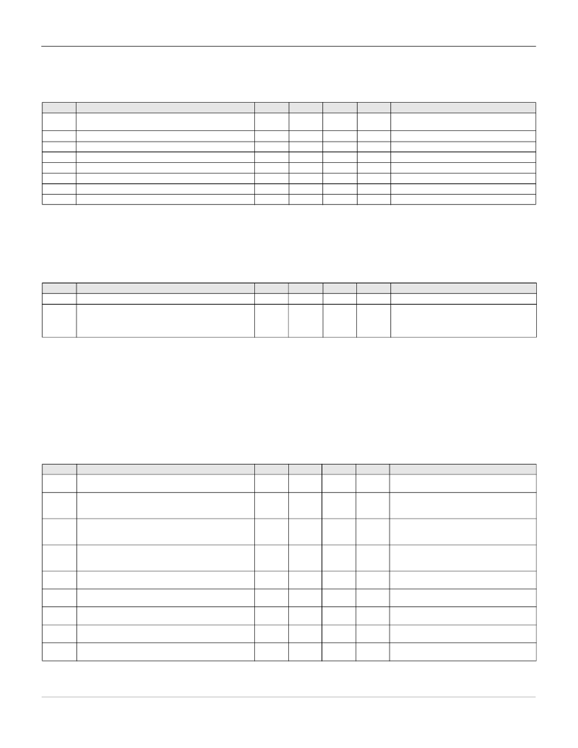
Table 3-2. Absolute Maximum Ratings
Symbol
T
STG
Description
Min
Typ
Max
Units
Notes
Storage Temperature
-55
–
+100
o
C
Higher storage temperatures will reduce data
retention time.
T
A
Vdd
V
IO
V
IOZ
I
MIO
ESD
LU
Ambient Temperature with Power Applied
Supply Voltage on Vdd Relative to Vss
DC Input Voltage
DC Voltage Applied to Tri-state
Maximum Current into any Port Pin
Electro Static Discharge Voltage
Latch-up Current
-40
-0.5
Vss - 0.5
Vss - 0.5
-25
2000
–
–
–
–
–
–
–
–
+85
+6.0
Vdd + 0.5 V
Vdd + 0.5 V
+50
–
200
o
C
V
mA
V
mA
Human Body Model ESD.
Table 3-3. Operating Temperature
Symbol
T
A
T
J
Description
Min
Typ
Max
Units
Notes
Ambient Temperature
Junction Temperature
-40
-40
–
–
+85
+100
o
C
o
C
The temperature rise from ambient to junction is
package specific. See
“Thermal Impedances”
on page 32
. The user must limit the power con-
sumption to comply with this requirement.
Table 3-4. DC Chip-Level Specifications
Symbol
Vdd
Description
Min
Typ
Max
Units
Notes
Supply Voltage
2.40
–
5.25
V
See table titled
“DC POR and LVD Specifica-
tions” on page 20
.
Conditions are Vdd = 5.0V, T
A
= 25
o
C, CPU = 3
MHz, 48 MHz disabled. VC1 = 1.5 MHz, VC2 =
93.75 kHz, VC3 = 0.366 kHz.
Conditions are Vdd = 3.3V, T
A
= 25
o
C, CPU = 3
MHz, clock doubler disabled. VC1 = 375 kHz,
VC2 = 23.4 kHz, VC3 = 0.091 kHz.
Conditions are Vdd = 2.55V, T
A
= 25
o
C, CPU = 3
MHz, clock doubler disabled. VC1 = 375 kHz,
VC2 = 23.4 kHz, VC3 = 0.091 kHz.
Vdd = 2.55V, 0
o
C
≤
T
A
≤
40
o
C.
I
DD
Supply Current, IMO = 24 MHz
–
3
4
mA
I
DD3
Supply Current, IMO = 6 MHz using SLIMO mode.
–
1.2
2
mA
I
DD27
Supply Current, IMO = 6 MHz using SLIMO mode.
–
1.1
1.5
mA
I
SB27
Sleep (Mode) Current with POR, LVD, Sleep Timer, WDT,
and internal slow oscillator active. Mid temperature range.
Sleep (Mode) Current with POR, LVD, Sleep Timer, WDT,
and internal slow oscillator active.
Reference Voltage (Bandgap)
–
2.6
4.
μ
A
I
SB
–
2.8
5
μ
A
Vdd = 3.3V, -40
o
C
≤
T
A
≤
85
o
C.
V
REF
1.28
1.30
1.32
V
Trimmed for appropriate Vdd. Vdd = 3.0V to
5.25V.
Trimmed for appropriate Vdd. Vdd = 2.4V to
3.0V.
V
REF27
Reference Voltage (Bandgap)
1.16
1.30
1.33
V
AGND
Analog Ground
V
REF
- 0.003
V
REF
V
REF
+ 0.003
V
相關PDF資料 |
PDF描述 |
|---|---|
| CY8C21434-24PVX | PSoC Mixed-Signal Array |
| CY8C21534-24PVX | PSoC Mixed-Signal Array |
| CY8C21234 | PSoC Mixed-Signal Array |
| CY8C21234-24AX | PSoC Mixed-Signal Array |
| CY8C21234-24C | PSoC Mixed-Signal Array |
相關代理商/技術參數(shù) |
參數(shù)描述 |
|---|---|
| CY8C21234-24PX | 制造商:CYPRESS 制造商全稱:Cypress Semiconductor 功能描述:PSoC Mixed-Signal Array |
| CY8C21234-24S | 制造商:CYPRESS 制造商全稱:Cypress Semiconductor 功能描述:PSoC㈢ Mixed-Signal Array |
| CY8C21234-24SX | 制造商:CYPRESS 制造商全稱:Cypress Semiconductor 功能描述:PSoC Mixed-Signal Array |
| CY8C2123424SXI | 制造商:Cypress Semiconductor 功能描述: |
| CY8C21234-24SXI | 功能描述:可編程片上系統(tǒng) - PSoC IC MCU 8K FLASH 512B SRAM RoHS:否 制造商:Cypress Semiconductor 核心:8051 處理器系列:CY8C36 數(shù)據(jù)總線寬度:8 bit 最大時鐘頻率:67 MHz 程序存儲器大小:32 KB 數(shù)據(jù) RAM 大小:4 KB 片上 ADC:Yes 工作電源電壓:0.5 V to 5.5 V 工作溫度范圍:- 40 C to + 85 C 封裝 / 箱體:QFN-68 安裝風格:SMD/SMT |
發(fā)布緊急采購,3分鐘左右您將得到回復。