- 您現(xiàn)在的位置:買賣IC網(wǎng) > PDF目錄378514 > CY8C21534-24PVX (Cypress Semiconductor Corp.) PSoC Mixed-Signal Array PDF資料下載
參數(shù)資料
| 型號(hào): | CY8C21534-24PVX |
| 廠商: | Cypress Semiconductor Corp. |
| 英文描述: | PSoC Mixed-Signal Array |
| 中文描述: | PSoC混合信號(hào)陣列 |
| 文件頁數(shù): | 1/35頁 |
| 文件大小: | 376K |
| 代理商: | CY8C21534-24PVX |
當(dāng)前第1頁第2頁第3頁第4頁第5頁第6頁第7頁第8頁第9頁第10頁第11頁第12頁第13頁第14頁第15頁第16頁第17頁第18頁第19頁第20頁第21頁第22頁第23頁第24頁第25頁第26頁第27頁第28頁第29頁第30頁第31頁第32頁第33頁第34頁第35頁
April 20, 2005
Cypress Semiconductor Corp. 2004-2005 — Document No. 38-12025 Rev. *G
1
PSoC Mixed-Signal Array
Final Data Sheet
CY8C21234, CY8C21334,
CY8C21434, CY8C21534, and CY8C21634
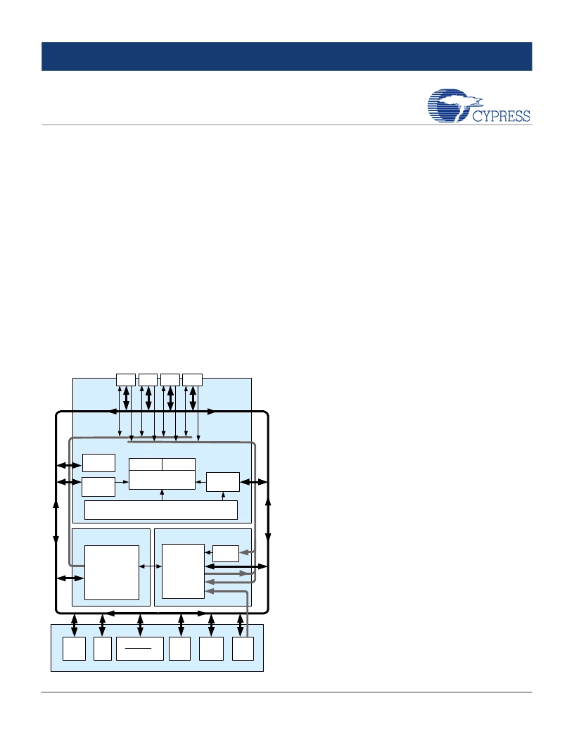
PSoC Functional Overview
The PSoC family consists of many
Mixed-Signal Array with
On-Chip Controller
devices. These devices are designed to
replace multiple traditional MCU-based system components
with one, low cost single-chip programmable component. A
PSoC device includes configurable blocks of analog and digital
logic, as well as programmable interconnect. This architecture
allows the user to create customized peripheral configurations,
to match the requirements of each individual application. Addi-
tionally, a fast CPU, Flash program memory, SRAM data mem-
ory, and configurable IO are included in a range of convenient
pinouts.
The PSoC architecture, as illustrated on the left, is comprised of
four main areas: the Core, the System Resources, the Digital
System, and the Analog System. Configurable global bus
resources allow all the device resources to be combined into a
complete custom system. Each CY8C21x34 PSoC device
includes four digital blocks and four analog blocks. Depending
on the PSoC package, up to 28 general purpose IO (GPIO) are
also included. The GPIO provide access to the global digital
and analog interconnects.
The PSoC Core
The PSoC Core is a powerful engine that supports a rich
instruction set. It encompasses SRAM for data storage, an
interrupt controller, sleep and watchdog timers, and IMO (inter-
nal main oscillator) and ILO (internal low speed oscillator). The
Features
■
Powerful Harvard Architecture Processor
M8C Processor Speeds to 24 MHz
Low Power at High Speed
2.4V to 5.25V Operating Voltage
Operating Voltages Down to 1.0V Using
On-Chip Switch Mode Pump (SMP)
Industrial Temperature Range: -40°C to +85°C
■
Advanced Peripherals (PSoC Blocks)
4 Analog Type “E” PSoC Blocks Provide:
- 2 Comparators with DAC Refs
- Single or Dual 8-Bit 28 Channel ADC
4 Digital PSoC Blocks Provide:
- 8- to 32-Bit Timers, Counters, and PWMs
- CRC and PRS Modules
- Full-Duplex UART, SPI
Master or Slave
- Connectable to All GPIO Pins
Complex Peripherals by Combining Blocks
■
Flexible On-Chip Memory
8K Flash Program Storage 50,000 Erase/Write
Cycles
512 Bytes SRAM Data Storage
In-System Serial Programming (ISSP
)
Partial Flash Updates
Flexible Protection Modes
EEPROM Emulation in Flash
■
Complete Development Tools
Free Development Software
(PSoC Designer)
Full-Featured, In-Circuit Emulator and
Programmer
Full Speed Emulation
Complex Breakpoint Structure
128K Trace Memory
■
Precision, Programmable Clocking
Internal ±2.5% 24/48 MHz Oscillator
Internal Oscillator for Watchdog and Sleep
■
Programmable Pin Configurations
25 mA Drive on All GPIO
Pull Up, Pull Down, High Z, Strong, or Open
Drain Drive Modes on All GPIO
Up to 8 Analog Inputs on GPIO
Configurable Interrupt on All GPIO
■
Versatile Analog Mux
Common Internal Analog Bus
Simultaneous Connection of IO Combinations
Capacitive Sensing Application Capability
■
Additional System Resources
I
2
C Master, Slave and Multi-Master to
400 kHz
Watchdog and Sleep Timers
User-Configurable Low Voltage Detection
Integrated Supervisory Circuit
On-Chip Precision Voltage Reference
DIGITAL SYSTEM
SRAM
512 Bytes
System Bus
Interrupt
Controller
Clock Sources
(Includes IMO and ILO)
Global Digital
Interconnect
Global Analog Interconnect
PSoC
CORE
CPU Core
(M8C)
SROM
Flash 8K
SYSTEM RESOURCES
ANALOG SYSTEM
Analog
Ref.
Digital
Clocks
I2C
POR and LVD
System Resets
Internal
Voltage
Ref.
Switch
Mode
Pump
Port 1
Port 0
Sleep and
Watchdog
Analog
Mux
Port 3
Port 2
Analog
PSoC
Block
Array
Digital
PSoC
Block
Array
相關(guān)PDF資料 |
PDF描述 |
|---|---|
| CY8C21234 | PSoC Mixed-Signal Array |
| CY8C21234-24AX | PSoC Mixed-Signal Array |
| CY8C21234-24C | PSoC Mixed-Signal Array |
| CY8C21234-24E | PSoC Mixed-Signal Array |
| CY8C21234-24I | PSoC Mixed-Signal Array |
相關(guān)代理商/技術(shù)參數(shù) |
參數(shù)描述 |
|---|---|
| CY8C21534-24PVXA | 功能描述:可編程片上系統(tǒng) - PSoC 24 I/O 8K Flash 512 bytes RAM RoHS:否 制造商:Cypress Semiconductor 核心:8051 處理器系列:CY8C36 數(shù)據(jù)總線寬度:8 bit 最大時(shí)鐘頻率:67 MHz 程序存儲(chǔ)器大小:32 KB 數(shù)據(jù) RAM 大小:4 KB 片上 ADC:Yes 工作電源電壓:0.5 V to 5.5 V 工作溫度范圍:- 40 C to + 85 C 封裝 / 箱體:QFN-68 安裝風(fēng)格:SMD/SMT |
| CY8C21534-24PVXAT | 功能描述:可編程片上系統(tǒng) - PSoC 24 I/O 8K Flash 512 bytes RAM RoHS:否 制造商:Cypress Semiconductor 核心:8051 處理器系列:CY8C36 數(shù)據(jù)總線寬度:8 bit 最大時(shí)鐘頻率:67 MHz 程序存儲(chǔ)器大小:32 KB 數(shù)據(jù) RAM 大小:4 KB 片上 ADC:Yes 工作電源電壓:0.5 V to 5.5 V 工作溫度范圍:- 40 C to + 85 C 封裝 / 箱體:QFN-68 安裝風(fēng)格:SMD/SMT |
| CY8C21534-24PVXI | 功能描述:可編程片上系統(tǒng) - PSoC IC MCU 8K FLASH 512B SRAM RoHS:否 制造商:Cypress Semiconductor 核心:8051 處理器系列:CY8C36 數(shù)據(jù)總線寬度:8 bit 最大時(shí)鐘頻率:67 MHz 程序存儲(chǔ)器大小:32 KB 數(shù)據(jù) RAM 大小:4 KB 片上 ADC:Yes 工作電源電壓:0.5 V to 5.5 V 工作溫度范圍:- 40 C to + 85 C 封裝 / 箱體:QFN-68 安裝風(fēng)格:SMD/SMT |
| CY8C21534-24PVXIT | 功能描述:可編程片上系統(tǒng) - PSoC 8K Flsh 512B RAM IND RoHS:否 制造商:Cypress Semiconductor 核心:8051 處理器系列:CY8C36 數(shù)據(jù)總線寬度:8 bit 最大時(shí)鐘頻率:67 MHz 程序存儲(chǔ)器大小:32 KB 數(shù)據(jù) RAM 大小:4 KB 片上 ADC:Yes 工作電源電壓:0.5 V to 5.5 V 工作溫度范圍:- 40 C to + 85 C 封裝 / 箱體:QFN-68 安裝風(fēng)格:SMD/SMT |
| CY8C21534-24PX | 制造商:CYPRESS 制造商全稱:Cypress Semiconductor 功能描述:PSoC Mixed-Signal Array |
發(fā)布緊急采購,3分鐘左右您將得到回復(fù)。