- 您現(xiàn)在的位置:買賣IC網(wǎng) > PDF目錄378513 > CY7C68023 (Cypress Semiconductor Corp.) EZ-USB NX2LP USB 2.0 NAND Flash Controller(EZ-USB NX2LP USB 2.0 NAND閃存控制器) PDF資料下載
參數(shù)資料
| 型號(hào): | CY7C68023 |
| 廠商: | Cypress Semiconductor Corp. |
| 英文描述: | EZ-USB NX2LP USB 2.0 NAND Flash Controller(EZ-USB NX2LP USB 2.0 NAND閃存控制器) |
| 中文描述: | 的EZ - USB NX2LP USB 2.0 NAND閃存控制器(的EZ - USB NX2LP的USB 2.0 NAND閃存控制器) |
| 文件頁(yè)數(shù): | 4/9頁(yè) |
| 文件大小: | 306K |
| 代理商: | CY7C68023 |
CY7C68023/CY7C68024
Document #: 38-08055 Rev. *B
Page 4 of 9
3.3
Additional Pin Descriptions
3.3.1
DPLUS and DMINUS are the USB signaling pins, and they
should be tied to the D+ and D– pins of the USB connector.
Because they operate at high frequencies, the USB signals
require special consideration when designing the layout of the
PCB. General guidelines are given at the end of this
document.
DPLUS, DMINUS
3.3.2
XTALIN, XTALOUT
The NX2LP requires a 24-MHz (±100 ppm) signal to derive
internal timing. Typically, a 24-MHz (20-pF, 500-
μ
W, parallel-
resonant fundamental mode) crystal is used, but a 24-MHz
square wave from another source can also be used. If a crystal
is used, connect its pins to XTALIN and XTALOUT, and also
through 12-pF capacitors to GND. If an alternate clock source
is used, apply it to XTALIN and leave XTALOUT open.
3.3.3
The Data[7-0] I/O pins provide an 8-bit interface to a NAND
Flash device. These pins are used to transfer address,
command, and read/write data between the NX2LP and NAND
Flash.
Data[7-0]
3.3.4
The Ready/Busy input pins are used to determine the state of
the currently selected NAND Flash device. These pins must
be pulled HIGH through a 2k-4k resistor. These pins are pulled
LOW by the NAND Flash when it is busy.
R_B[2-1]#
3.3.5
The Write Enable output pin is used by the NAND Flash to
latch commands, address, and data during the rising edge of
the pulse.
WE#
3.3.6
The Read Enable output pins are used to control the data flow
from the NAND Flash devices. The device presents valid data
and will increment its internal column address counter by one
RE[1-0]#
step on each falling edge of the Read Enable pulse. A 10k pull-
up is an option For RE1-0#.
3.3.7
The Command Latch Enable output pin is used to indicate that
the data on the I/O bus is a command. The data is latched into
the NAND Flash control register on the rising edge of WE#
when CLE is HIGH.
CLE
3.3.8
The Address Latch Enable output pin is used to indicate that
the data on the I/O bus is an address. The data is latched into
the NAND Flash address register on the rising edge of WE#
when ALE is HIGH.
ALE
3.3.9
The Data Activity LED output pin is used to indicate data
transfer activity. LED1# is asserted LOW at the beginning of a
data transfer, and set to a high-Z state when the transfer is
complete. If this functionality is not utilized, leave LED1#
floating.
LED1#
3.3.10
The Chip Active LED output pin is used to indicate proper
device operation. LED2# is asserted LOW when the NX2LP is
powered and initialized. It is placed in a high-Z state under all
other conditions. If this functionality is not utilized, leave
LED2# floating.
LED2#
3.3.11
The Write-protect NAND Flash output pin is used to control the
write-protect pins on NAND Flash devices. This pin should be
tied to the Write Protect pins of the NAND Flash devices. If
WP_SW# is asserted LOW during a data transfer, or if internal
operations are still pending, the NX2LP will wait until the
operation is complete before asserting WP_NF# to ensure that
there is no data loss or risk of OS error.
WP_NF#
3.3.12
The Write-protect Switch input pin is used to select whether or
not NAND Flash write-protection is enabled by the NX2LP.
When the pin is asserted LOW, the NX2LP will report to the
host that the NAND Flash is write-protected, the WP_NF# will
be driven LOW, and any attempts to write to the configuration
data memory area will be blocked by the NX2LP. If this pin is
asserted LOW during a data transfer, or if internal operations
are still pending, the NX2LP will wait until the operation is
complete before asserting WP_NF# to ensure that there is no
data loss or risk of OS error.
WP_SW#
3.3.13
The Chip Enable output pins are used to select the NAND
Flash that the NX2LP will interface. Unused Chip Enable pins
should be left floating.
CE[7-0]#
3.3.14
Asserting RESET# for 10 ms will reset the NX2LP. A reset
and/or watchdog chip is recommended to ensure that startup
and brownout conditions are properly handled.
RESET#
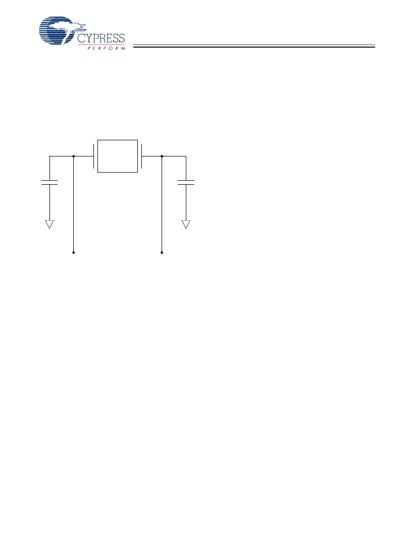
Figure 3-2. XTALIN, XTALOUT Diagram
24-MHz Xtal
12 pF
XTALIN
XTALOUT
12 pF
12-pF capacitor
values assume a
trace capacitance
of 3 pF per side on a
four-layer FR4 PCB
相關(guān)PDF資料 |
PDF描述 |
|---|---|
| CY7C9235A | SMPTE-259M/DVB-ASI Scrambler/Controller(SMPTE-259M/DVB-ASI擾頻器/控制器) |
| CY7C924ADX | 200 MBaud HOTLink Transceiver(200MBaud HOTLink收發(fā)器) |
| CY7C924DX | 200-MBaud HOTLink Transceiver(200H波特?zé)峤硬迨瞻l(fā)器) |
| CY7C954DX | ATM HOTLink Transceiver(ATM 熱接插收發(fā)器) |
| CY7C964A | Bus Interface Logic Circuit |
相關(guān)代理商/技術(shù)參數(shù) |
參數(shù)描述 |
|---|---|
| CY7C68023-56BAXC | 功能描述:IC USB NX2LP NAND CNTRLR 56VFBGA RoHS:是 類別:集成電路 (IC) >> 接口 - 控制器 系列:CY7C 標(biāo)準(zhǔn)包裝:4,900 系列:- 控制器類型:USB 2.0 控制器 接口:串行 電源電壓:3 V ~ 3.6 V 電流 - 電源:135mA 工作溫度:0°C ~ 70°C 安裝類型:表面貼裝 封裝/外殼:36-VFQFN 裸露焊盤 供應(yīng)商設(shè)備封裝:36-QFN(6x6) 包裝:* 其它名稱:Q6396337A |
| CY7C68023-56LFXC | 功能描述:USB 接口集成電路 EZ USB NX2LPT USB2.0 Flash Controllr COM RoHS:否 制造商:Cypress Semiconductor 產(chǎn)品:USB 2.0 數(shù)據(jù)速率: 接口類型:SPI 工作電源電壓:3.15 V to 3.45 V 工作電源電流: 最大工作溫度:+ 85 C 安裝風(fēng)格:SMD/SMT 封裝 / 箱體:WLCSP-20 |
| CY7C68023-56LTXC | 功能描述:USB 接口集成電路 EZ-USB NX2LP NAND Flash Controller RoHS:否 制造商:Cypress Semiconductor 產(chǎn)品:USB 2.0 數(shù)據(jù)速率: 接口類型:SPI 工作電源電壓:3.15 V to 3.45 V 工作電源電流: 最大工作溫度:+ 85 C 安裝風(fēng)格:SMD/SMT 封裝 / 箱體:WLCSP-20 |
| CY7C68023-56LTXCKM | 制造商:Rochester Electronics LLC 功能描述: 制造商:Cypress Semiconductor 功能描述: |
| CY7C68023-56LTXCT | 制造商:Cypress Semiconductor 功能描述:USB - Tape and Reel 制造商:Cypress Semiconductor 功能描述:IC MEMORY CONTROLLERS 制造商:Cypress Semiconductor 功能描述:Async Fast SRAMs |
發(fā)布緊急采購(gòu),3分鐘左右您將得到回復(fù)。