- 您現(xiàn)在的位置:買賣IC網(wǎng) > PDF目錄378513 > CY7C63001C (Cypress Semiconductor Corp.) Universal Serial Bus Microcontroller(通用串行總線微控制器) PDF資料下載
參數(shù)資料
| 型號(hào): | CY7C63001C |
| 廠商: | Cypress Semiconductor Corp. |
| 英文描述: | Universal Serial Bus Microcontroller(通用串行總線微控制器) |
| 中文描述: | 通用串行總線控制器(通用串行總線微控制器) |
| 文件頁(yè)數(shù): | 13/28頁(yè) |
| 文件大?。?/td> | 1076K |
| 代理商: | CY7C63001C |
第1頁(yè)第2頁(yè)第3頁(yè)第4頁(yè)第5頁(yè)第6頁(yè)第7頁(yè)第8頁(yè)第9頁(yè)第10頁(yè)第11頁(yè)第12頁(yè)當(dāng)前第13頁(yè)第14頁(yè)第15頁(yè)第16頁(yè)第17頁(yè)第18頁(yè)第19頁(yè)第20頁(yè)第21頁(yè)第22頁(yè)第23頁(yè)第24頁(yè)第25頁(yè)第26頁(yè)第27頁(yè)第28頁(yè)
CY7C63001C
CY7C63101C
Document #: 38-08026 Rev. *B
Page 13 of 28
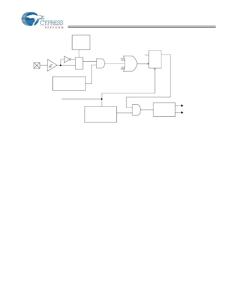
Note:
If one port pin triggers an interrupt, no other port pin can
cause a GPIO interrupt until the port pin that triggered the
interrupt has returned to its inactive (non-trigger) state or until
its corresponding port interrupt enable bit is cleared (these
events ‘reset’ the clock of the GPIO Interrupt flip-flop, which
must be ‘reset’ to ‘0’ before another GPIO interrupt event can
‘clock’ the GPIO Interrupt flip-flop and produce an IRQ).
Note:
If the port pin that triggered an interrupt is held in its
active (trigger) state while its corresponding port interrupt
enable bit is cleared and then set, a GPIO interrupt event
occurs as the GPIO Interrupt flip-flop clock transitions from ‘1’
to ‘0’ and then back to ‘1’ (please refer to
Figure 6-16
). The
USB Controller does not assign interrupt priority to different
port pins and the Port Interrupt Enable Registers are not
cleared during the interrupt acknowledge process. When a
GPIO interrupt is serviced, the ISR must poll the ports to
determine which pin caused the interrupt.
6.8.3
A USB Endpoint 0 interrupt is generated after the host has
written data to Endpoint 0 or after the USB Controller has
transmitted a packet from Endpoint 0 and receives an ACK
from the host. An OUT packet from the host which is NAKed
by the USB Controller does not generate an interrupt. This
interrupt is masked by the USB EP0 Interrupt Enable bit (bit 3)
of the Global Interrupt Enable Register.
A USB Endpoint 1 interrupt is generated after the USB
Controller has transmitted a packet from Endpoint 1 and has
received an ACK from the host. This interrupt is masked by the
USB EP1 Interrupt Enable bit (bit 4) of the Global Interrupt
Enable Register.
USB Interrupt
6.8.4
There are two timer interrupts: the 128-
μ
s interrupt and the
1.024-ms interrupt. They are masked by bits 1 and 2 of the
Global Interrupt Enable Register respectively. The user should
disable both timer interrupts before going into the suspend
Timer Interrupt
mode to avoid possible conflicts from timer interrupts occurring
just as suspend mode is entered.
6.8.5
A wake-up interrupt is generated when the Cext pin goes
HIGH. This interrupt is latched in the interrupt controller. It can
be masked by the Wake-up Interrupt Enable bit (bit 7) of the
Global Interrupt Enable Register. This interrupt can be used to
perform periodic checks on attached peripherals when the
USB Controller is placed in the low-power suspend mode. See
the Instant-On Feature section for more details.
Wake-Up Interrupt
6.9
The USB engine includes the Serial Interface Engine (SIE)
and the low-speed USB I/O transceivers. The SIE block
performs most of the USB interface functions with only minimal
support from the microcontroller core. Two endpoints are
supported. Endpoint 0 is used to receive and transmit control
(including setup) packets while Endpoint 1 is only used to
transmit data packets.
The USB SIE processes USB bus activity at the transaction
level independently. It does all the NRZI encoding/decoding
and bit stuffing/unstuffing. It also determines token type,
checks address and endpoint values, generates and checks
CRC values, and controls the flow of data bytes between the
bus and the Endpoint FIFOs. NOTE: the SIE stalls the CPU for
3 cycles per byte when writing data to the endpoint FIFOs (or
3 * 1/12 MHz * 8 bytes = 2
μ
s per 8-byte transfer).
The firmware handles higher level and function-specific tasks.
During control transfers the firmware must interpret device
requests and respond correctly. It also must coordinate
Suspend/Resume, verify and select DATA toggle values, and
perform function specific tasks.
The USB engine and the firmware communicate though the
Endpoint FIFOs, USB Endpoint interrupts, and the USB
registers described in the sections below.
USB Engine
Figure 6-16. GPIO Interrupt Logic Block Diagram
Port
Pull-Up
Register
1=L
→
H
0=H
→
L
OR Gate
(1 input per
GPIO pin)
GPIO Interrupt
Flip-Flop
CLR
GPIO
Pin
1 = Enable
0 = Disable
Port Interrupt
Enable Register
1 = Enable
0 = Disable
Interrupt
Acknowledge
Interrupt
Priority
Encoder
IRQ
Interrupt
Vector
D
Q
CLR
M
U
X
I
Global
GPIO Interrupt
Enable
(Bit 6, Register 0x20)
相關(guān)PDF資料 |
PDF描述 |
|---|---|
| CY7C63231-PC | enCoRe USB Low-speed USB Peripheral Controller |
| CY7C63231A-SC | enCoRe USB Low-speed USB Peripheral Controller |
| CY7C63221A | enCoRe USB Low-speed USB Peripheral Controller |
| CY7C63221A-PC | enCoRe USB Low-speed USB Peripheral Controller |
| CY7C63221A-XC | TV 32C 32#20 SKT RECP |
相關(guān)代理商/技術(shù)參數(shù) |
參數(shù)描述 |
|---|---|
| CY7C63001C-PXC | 功能描述:8位微控制器 -MCU Universal Serial Bus Microcontroller RoHS:否 制造商:Silicon Labs 核心:8051 處理器系列:C8051F39x 數(shù)據(jù)總線寬度:8 bit 最大時(shí)鐘頻率:50 MHz 程序存儲(chǔ)器大小:16 KB 數(shù)據(jù) RAM 大小:1 KB 片上 ADC:Yes 工作電源電壓:1.8 V to 3.6 V 工作溫度范圍:- 40 C to + 105 C 封裝 / 箱體:QFN-20 安裝風(fēng)格:SMD/SMT |
| CY7C63001C-SC | 制造商:Cypress Semiconductor 功能描述: |
| CY7C63001C-SXC | 功能描述:8位微控制器 -MCU Universal Serial Bus Microcontroller RoHS:否 制造商:Silicon Labs 核心:8051 處理器系列:C8051F39x 數(shù)據(jù)總線寬度:8 bit 最大時(shí)鐘頻率:50 MHz 程序存儲(chǔ)器大小:16 KB 數(shù)據(jù) RAM 大小:1 KB 片上 ADC:Yes 工作電源電壓:1.8 V to 3.6 V 工作溫度范圍:- 40 C to + 105 C 封裝 / 箱體:QFN-20 安裝風(fēng)格:SMD/SMT |
| CY7C63001C-SXCT | 功能描述:8位微控制器 -MCU USB Microcontroller RoHS:否 制造商:Silicon Labs 核心:8051 處理器系列:C8051F39x 數(shù)據(jù)總線寬度:8 bit 最大時(shí)鐘頻率:50 MHz 程序存儲(chǔ)器大小:16 KB 數(shù)據(jù) RAM 大小:1 KB 片上 ADC:Yes 工作電源電壓:1.8 V to 3.6 V 工作溫度范圍:- 40 C to + 105 C 封裝 / 箱體:QFN-20 安裝風(fēng)格:SMD/SMT |
| CY7C63001C-XC DIE | 制造商:Cypress Semiconductor 功能描述: |
發(fā)布緊急采購(gòu),3分鐘左右您將得到回復(fù)。