- 您現(xiàn)在的位置:買賣IC網(wǎng) > PDF目錄378513 > CY7C4841 (Cypress Semiconductor Corp.) 4K x9 x2 Double Sync FIFOs(4K x9 x2 雙路同步先進(jìn)先出) PDF資料下載
參數(shù)資料
| 型號: | CY7C4841 |
| 廠商: | Cypress Semiconductor Corp. |
| 英文描述: | 4K x9 x2 Double Sync FIFOs(4K x9 x2 雙路同步先進(jìn)先出) |
| 中文描述: | 4K的X9熱賣x2雙同步FIFO的(4K的X9熱賣x2雙路同步先進(jìn)先出) |
| 文件頁數(shù): | 4/22頁 |
| 文件大小: | 348K |
| 代理商: | CY7C4841 |
CY7C4801/4811/4821
CY7C4831/4841/4851
4
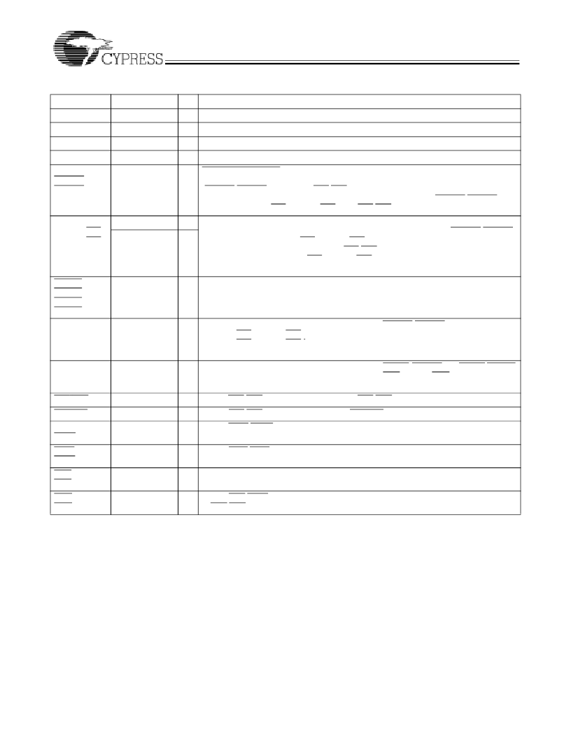
Pin Definitions
Signal Name
Description
I/O
Description
DA
0
8
DB
0
8
QA
0
8
QB
0
8
Data Inputs
I
Data Inputs for 9-bit bus
Data Inputs
I
Data Inputs for 9-bit bus
Data Outputs
O
Data Outputs for 9-bit bus
Data Outputs
O
Data Outputs for 9-bit bus
WENA1
WENB1
Write Enable 1
I
WENA1 and WENB1become the only write enables when the device is configured to
have programmable flags. Data is written on a LOW-to-HIGH transition of WCLK when
(WENA1,WENB1) is LOW and (FFA,FFB) is HIGH. If the FIFO is configured to have two write
enables, data is written on a LOW-to-HIGH transition of WCLK when (WENA1,WENB1) is
LOW and (WENA2/LDA,WENB2/LDB) and (FFA,FFB) are HIGH.
WENA2/LDA
WENB2/LDB
Dual Mode Pin
Write Enable 2
I
If HIGH at reset, this pin operates as a second write enable. If LOW at reset, this pin
operates as a control to write or read the programmable flag offsets. (WENA1,WENB1)
must be LOW and (WENA2/LDA,WENB2/LDB) must be HIGH to write data into the FIFO.
Data will not be written into the FIFO if the (FFA,FFB) is LOW. If the FIFO is configured to have
programmable flags, (WENA2/LDA,WENB2/LDB) is held LOW to write or read the program-
mable flag offsets.
Load
I
RENA1
RENA2
RENB1
RENB2
Read Enable
Inputs
I
Enables the device for Read operation.
WCLKA
WCKLB
Write Clock
I
The rising edge clocks data into the FIFO when (WENA1,WENB1) is LOW and
(WENA2/LDA,WENB2/LDB) is HIGH and the FIFO is not Full. When
(WENA2/LDA,WENB2/LDB) is asserted, WCLK writes data into the programmable flag-offset
register.
RCLKA
RCLKB
Read Clock
I
The rising edge clocks data out of the FIFO when (RENA1 ,RENB1) and (RENA2,RENB2)
are LOW and the FIFO is not Empty. When (WENA2/LDA,WENB2/LDB) is LOW,
(RCLKA,RCLKB) reads data out of the programmable flag-offset register.
EFA,EFB
Empty Flag
O
When (EFA,EFB) is LOW, the FIFO is empty. (EFA,EFB) is synchronized to (RCLKA,RCLKB).
FFA,FFB
Full Flag
O
When (FFA,FFB) is LOW, the FIFO is full. (FFA,FFB) is synchronized to (WCLKA,WCLKB).
PAEA
PAEB
Programmable
Almost Empty
O
When (PAEA,PAEB) is LOW, the FIFO is almost empty based on the almost empty offset value
programmed into the FIFO. PAE is synchronized to RCLK.
PAFA
PAFB
Programmable
Almost Full
O
When (PAFA,PAFB) is LOW, the FIFO is almost full based on the almost full offset value pro-
grammed into the FIFO. PAF is synchronized to WCLK.
RSA
RSB
Reset
I
Resets device to empty condition. A reset is required before an initial read or write
operation after power-up.
OEA
OEB
Output Enable
I
When (OEA,OEB) is LOW, the FIFO’s data outputs drive the bus to which they are connected.
If (OEA,OEB) is HIGH, the FIFO’s outputs are in High Z (high-impedance) state.
相關(guān)PDF資料 |
PDF描述 |
|---|---|
| CY7C60113 | Wireless enCoRe II Microcontroller(無線enCoRe II微控制器) |
| CY7C60123 | Wireless enCoRe II Microcontroller(無線enCoRe II微控制器) |
| CY7C60223 | Wireless enCoRe II Microcontroller(無線enCoRe II微控制器) |
| CY7C60333 | enCoRe III Low Voltage(enCoRe III低電壓) |
| CY7C60323 | enCoRe III Low Voltage(enCoRe III低電壓) |
相關(guān)代理商/技術(shù)參數(shù) |
參數(shù)描述 |
|---|---|
| CY7C4841-15AC | 制造商:Cypress Semiconductor 功能描述:FIFO Mem Sync Quad Depth/Width Bi-Dir 4K x 9 x 2 64-Pin TQFP 制造商:Rochester Electronics LLC 功能描述:4K X9 X2 DOUBLE SYNC FIFO - Bulk |
| CY7C4851-10AC | 制造商:Cypress Semiconductor 功能描述:FIFO Mem Sync Quad Depth/Width Bi-Dir 8K x 9 x 2 64-Pin TQFP 制造商:Rochester Electronics LLC 功能描述:8K X9 X2 DOUBLE SYNC FIFO - Bulk |
| CY7C510 | 制造商: 功能描述: 制造商:Cypress Semiconductor 功能描述: 制造商:undefined 功能描述: |
| CY7C510-55GMB | 制造商: 功能描述: 制造商:undefined 功能描述: |
| CY7C51055LMB | 制造商:CYPRESS 功能描述:IC |
發(fā)布緊急采購,3分鐘左右您將得到回復(fù)。