- 您現(xiàn)在的位置:買賣IC網(wǎng) > PDF目錄379092 > CY7C4241 (Cypress Semiconductor Corp.) 4K x 9 Synchronous FIFOs(4Kx9同步先進(jìn)先出(FIFO)) PDF資料下載
參數(shù)資料
| 型號(hào): | CY7C4241 |
| 廠商: | Cypress Semiconductor Corp. |
| 英文描述: | 4K x 9 Synchronous FIFOs(4Kx9同步先進(jìn)先出(FIFO)) |
| 中文描述: | 4K的× 9(4Kx9同步先進(jìn)先出(FIFO)的同步FIFO的) |
| 文件頁數(shù): | 1/19頁 |
| 文件大小: | 550K |
| 代理商: | CY7C4241 |
64/256/512/1K/2K/4K/8K x 9 Synchronous FIFOs
CY7C4421/4201/4211/4221
CY7C4231/4241/4251
Cypress Semiconductor Corporation
Document #: 38-06016 Rev. *C
3901 North First Street
San Jose
,
CA 95134
408-943-2600
Revised August 2, 2005
Features
High-speed, low-power, First-In, First-Out (FIFO)
memories
— 64 × 9 (CY7C4421)
— 256 × 9 (CY7C4201)
— 512 × 9 (CY7C4211)
— 1K × 9 (CY7C4221)
— 2K × 9 (CY7C4231)
— 4K × 9 (CY7C4241)
— 8K × 9 (CY7C4251)
High-speed 100-MHz operation (10 ns Read/Write cycle
time)
Low power (I
CC
= 35 mA)
Fully asynchronous and simultaneous Read and Write
operation
Empty, Full, and Programmable Almost Empty and
Almost Full status flags
TTL-compatible
Expandable in width
Output Enable (OE) pin
Independent Read and Write enable pins
Center power and ground pins for reduced noise
Width-expansion capability
Space saving 7 mm × 7 mm 32-pin TQFP
Pin-compatible and functionally equivalent to
IDT72421, 72201, 72211, 72221, 72231, and 72241
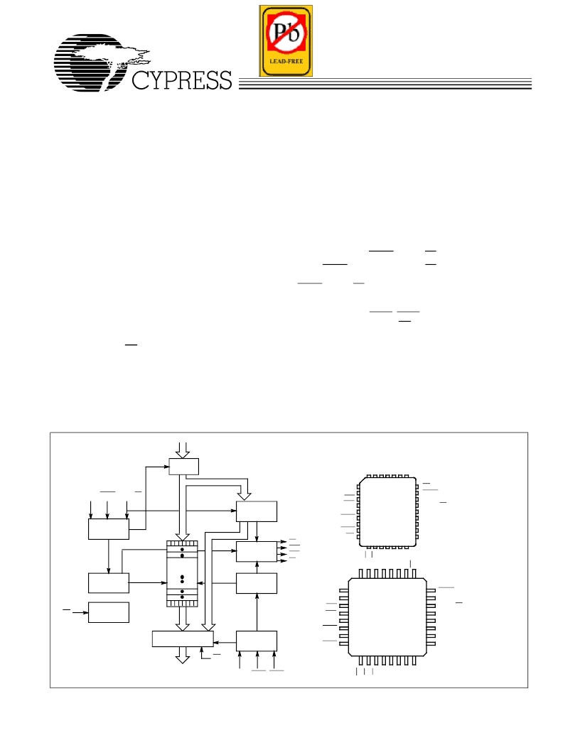
Logic Block Diagram
Pb-Free Packages Available
Functional Description
The CY7C42X1 are high-speed, low-power FIFO memories
with clocked Read and Write interfaces. All are 9 bits wide. The
CY7C42X1 are pin-compatible to IDT722X1. Programmable
features include Almost Full/Almost Empty flags. These FIFOs
provide solutions for a wide variety of data buffering needs,
including high-speed data acquisition, multiprocessor inter-
faces, and communications buffering.
These FIFOs have 9-bit input and output ports that are
controlled by separate clock and enable signals. The input port
is controlled by a free-running clock (WCLK) and two
Write-enable pins (WEN1, WEN2/LD).
When WEN1 is LOW and WEN2/LD is HIGH, data is written
into the FIFO on the rising edge of the WCLK signal. While
WEN1, WEN2/LD is held active, data is continually written into
the FIFO on each WCLK cycle. The output port is controlled in
a similar manner by a free-running Read clock (RCLK) and two
Read-enable pins (REN1, REN2). In addition, the CY7C42X1
has an output enable pin (OE). The Read (RCLK) and Write
(WCLK) clocks may be tied together for single-clock operation
or the two clocks may be run independently for asynchronous
Read/Write applications. Clock frequencies up to 100 MHz are
achievable.
Depth expansion is possible using one enable input for system
control, while the other enable is controlled by expansion logic
to direct the flow of data.
Pin Configurations
THREE-STATE
OUTPUT REGISTER
Read
CONTROL
FLAG
LOGIC
Write
CONTROL
Write
POINTER
Read
POINTER
RESET
LOGIC
INPUT
REGISTER
FLAG
PROGRAM
REGISTER
D0- 8
RCLK
EF
PAE
PAF
FF
Q0- 8
WEN1
WCLK
RS
OE
D64 x 9
8k x 9
WEN2/LD
REN1 REN2
D
8
D
7
D
6
D
5
D
4
D
3
D
2
1
2
3
4
5
6
7
8
D
1
D
0
RCLK
REN2
GND
REN1
PAF
PAE
17
18
19
20
21
22
23
24
14 15 16
9 10 11 1213
31 30
32
2928 27
25
26
F
Q
0
Q
1
Q
2
Q
3
Q
4
E
O
V
CC
Q
8
Q
7
Q
6
Q
5
WCLK
WEN2/LD
WEN1
R
TTQFP
PLCC
Top View
D
1
D
0
RCLK
REN2
V
CC
Q
8
Q
7
Q
6
Q
5
D
8
D
7
D
6
D
5
D
4
D
3
GND
REN1
WCLK
WEN2/LD
D
2
PAF
5
6
7
8
9
10
11
12
13
OE
4 3 2 1
3130
32
21
22
23
24
27
26
28
29
25
14151617181920
WEN1
RS
F
Q
0
Q
1
Q
2
Q
3
Q
4
E
CY7C4421/4201/4211/4221
CY7C4231/4241/425164/256/512/1K/2K/4K/8K x 9 Synchronous FIFOs
相關(guān)PDF資料 |
PDF描述 |
|---|---|
| CY7C4421 | 64× 9 Synchronous FIFOs(64×9同步先進(jìn)先出(FIFO)) |
| CY7C4231 | 2K x 9 Synchronous FIFOs(2Kx9同步先進(jìn)先出(FIFO)) |
| CY7C4251 | 8K x 9 Synchronous FIFOs(8Kx9同步先進(jìn)先出(FIFO)) |
| CY7C4235-25ASI | 64/256/512/1K/2K/4K x18 Low-Voltage Synchronous FIFOs |
| CY7C4225V-15AC | OSC 5V SMT 7X5 CMOS PROGRM |
相關(guān)代理商/技術(shù)參數(shù) |
參數(shù)描述 |
|---|---|
| CY7C4241 WAF | 制造商:Cypress Semiconductor 功能描述: |
| CY7C4241-10AC | 制造商:Cypress Semiconductor 功能描述:FIFO Mem Sync Dual Depth/Width Uni-Dir 4K x 9 32-Pin TQFP 制造商:Rochester Electronics LLC 功能描述:4K X 9 32 PIN IDT COMPAT SYNCH FIFO - Bulk |
| CY7C4241-10ACT | 制造商:Cypress Semiconductor 功能描述: |
| CY7C4241-10AXC | 功能描述:先進(jìn)先出 4Kx9 IDT Compat SYNC 先進(jìn)先出 COM RoHS:否 制造商:IDT 電路數(shù)量: 數(shù)據(jù)總線寬度:18 bit 總線定向:Unidirectional 存儲(chǔ)容量:4 Mbit 定時(shí)類型:Synchronous 組織:256 K x 18 最大時(shí)鐘頻率:100 MHz 訪問時(shí)間:10 ns 電源電壓-最大:3.6 V 電源電壓-最小:6 V 最大工作電流:35 mA 最大工作溫度:+ 85 C 封裝 / 箱體:TQFP-80 封裝: |
| CY7C4241-10AXCT | 功能描述:先進(jìn)先出 4Kx9 IDT Compat SYNC 先進(jìn)先出 COM RoHS:否 制造商:IDT 電路數(shù)量: 數(shù)據(jù)總線寬度:18 bit 總線定向:Unidirectional 存儲(chǔ)容量:4 Mbit 定時(shí)類型:Synchronous 組織:256 K x 18 最大時(shí)鐘頻率:100 MHz 訪問時(shí)間:10 ns 電源電壓-最大:3.6 V 電源電壓-最小:6 V 最大工作電流:35 mA 最大工作溫度:+ 85 C 封裝 / 箱體:TQFP-80 封裝: |
發(fā)布緊急采購,3分鐘左右您將得到回復(fù)。