- 您現(xiàn)在的位置:買賣IC網(wǎng) > PDF目錄379092 > CY7C409A (Cypress Semiconductor Corp.) 64 x 9 Cascadable FIFO(64 x 9位級聯(lián)型先進先出(FIFO)) PDF資料下載
參數(shù)資料
| 型號: | CY7C409A |
| 廠商: | Cypress Semiconductor Corp. |
| 英文描述: | 64 x 9 Cascadable FIFO(64 x 9位級聯(lián)型先進先出(FIFO)) |
| 中文描述: | 64 × 9級聯(lián)的FIFO(64 × 9位級聯(lián)型先進先出(FIFO)的) |
| 文件頁數(shù): | 8/16頁 |
| 文件大?。?/td> | 280K |
| 代理商: | CY7C409A |
CY7C408A
CY7C409A
8
Architecture of the CY7C408A and CY7C409A
The CY7C408A and CY7C409A FIFOs consist of an array of
64 words of 8 or 9 bits each (which are implemented using a
dual-port RAM cell), a write pointer, a read pointer, and the
control logic necessary to generate the handshaking (SI/IR,
SO/OR) signals as well as the almost full/almost empty (AFE)
and half full (HF) flags. The handshaking signals operate in a
manner identical to those of the industry standard
CY7C401/402/403/404 FIFOs.
Dual-Port RAM
The dual-port RAM architecture refers to the basic memory
cell used in the RAM. The cell itself enables the read and write
operations to be independent of each other, which is neces-
sary to achieve truly asynchronous operation of the inputs and
outputs. A second benefit is that the time required to increment
the read and write pointers is much less than the time that
would be required for data to propagate through the memory,
which it would have to do if the memory were implemented
using the conventional register array architecture.
Fall-Through and Bubble-Back
The time required for data to propagate from the input to the
output of an initially empty FIFO is defined as the fall-through
time.
The time required for an empty location to propagate from the
output to the input of an initially full FIFO is defined as the
bubble-back time.
The maximum rate at which data can be passed through the
FIFO (called the throughput) is limited by the fall-through time
when it is empty (or near empty) and by the bubble-back time
when it is full (or near full).
The conventional definitions of fall-through and bubble-back
do not apply to the CY7C408A and CY7C409A FIFOs be-
cause the data does not physically propagate through the
memory. The read and write pointers are incremented instead
of moving the data. However, the parameter is specified be-
cause it does represent the worst-case propagation delay for
the control signals. That is, the time required to increment the
write pointer and propagate a signal from the SI input to the
OR output of an empty FIFO or the time required to increment
the read pointer and propagate a signal from the SO input to
the IR output of a full FIFO.
Resetting the FIFO
Upon power-up, the FIFO must be reset with a master reset
(MR) signal. This causes the device to enter the empty condi-
tion, which is signified by the OR signal being LOW at the
same time that the IR signal is HIGH. In this condition, the data
outputs (DO
0
– DO
8
) will be LOW. The AFE flag will be HIGH
and the HF flag will be LOW.
Shifting Data Into the FIFO
The availability of an empty location is indicated by the HIGH
state of the input ready (IR) signal. When IR is HIGH a LOW
to HIGH transition on the shift in (SI) pin will clock the data on
the DI
0
- DI
8
inputs into the FIFO. Data propagates through the
device at the falling edge of SI.
The IR output will then go LOW, indicating that the data has
been sampled. The HIGH-to-LOW transition of the SI signal
initiates the LOW-to-HIGH transition of the IR signal if the FIFO
is not full. If the FIFO is full, IR will remain LOW.
Shifting Data Out of the FIFO
The availability of data at the outputs of the FIFO is indicated
by the HIGH state of the output ready (OR) signal. After the
FIFO is reset all data outputs (DO
0
– DO
8
) will be in the LOW
state. As long as the FIFO remains empty, the OR signal will
be LOW and all SO pulses applied to it will be ignored. After
data is shifted into the FIFO, the OR signal will go HIGH. The
external control logic (designed by the user) should use the
HIGH state of the OR signal to generate a SO pulse. The data
outputs of the FIFO should be sampled with edge-sensitive
type D flip-flops (or equivalent), using the SO signal as the
clock input to the flip-flop.
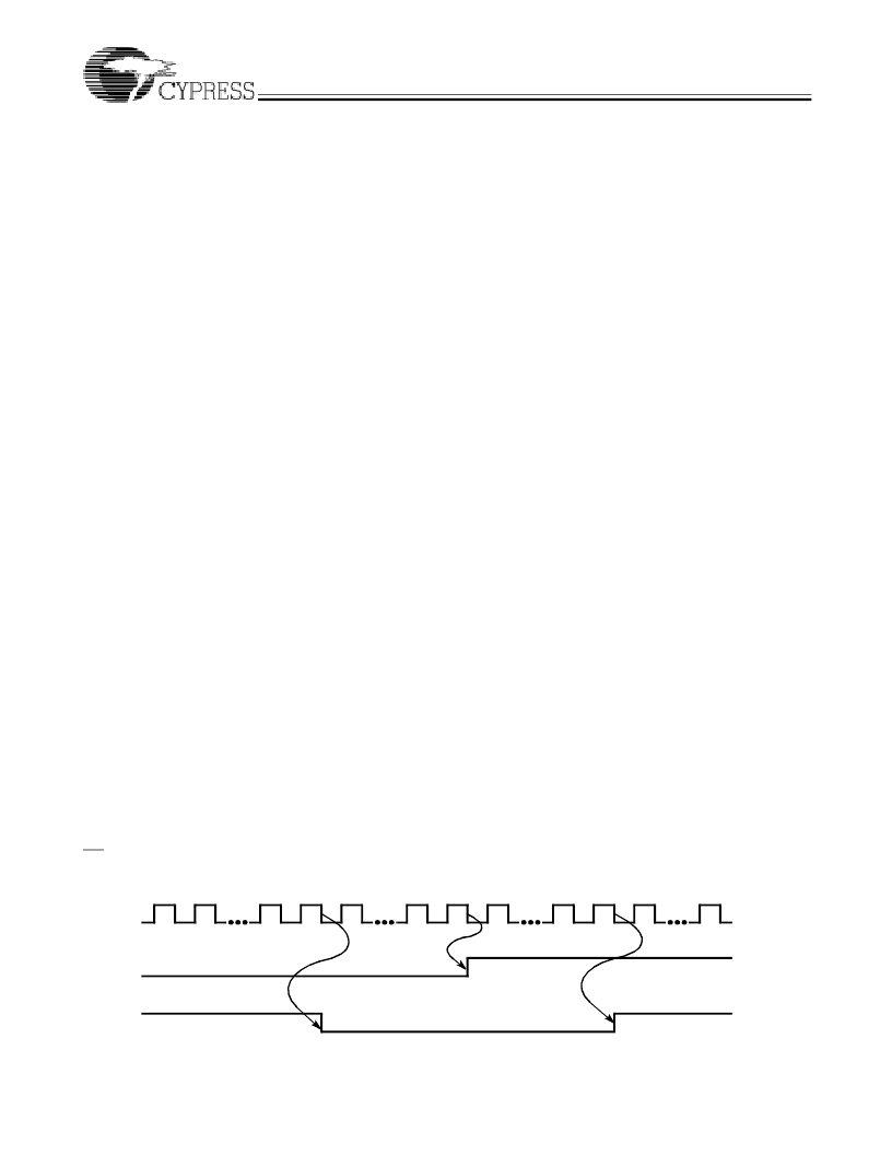
AFE and HF Flags
Two flags, almost full/almost empty (AFE) and half full (HF),
describe how many words are stored in the FIFO. AFE is HIGH
when there are 8 or fewer or 56 or more words stored in the
FIFO. Otherwise the AFE flag is LOW. HF is HIGH when there
are 32 or more words stored in the FIFO, otherwise the HF flag
is LOW. Flag transitions occur relative to the falling edges of
SI and SO (Figures 1 and 2).
Due to the asynchronous nature of the SI and SO signals, it is
possible to encounter specific timing relationships which may
cause short pulses on the AFE and HF flags. These pulses are
entirely due to the dynamic relationship of the SI and SO sig-
nals. The flags, however, will always settle to their correct state
after the appropriate delay (t
DHAFE
, t
DLAFE
, t
DHHF
, or t
DLHF
).
Therefore, use of level-sensitive rather than edge-sensitive
flag detection devices is recommended to avoid false flag en-
coding.
Figure 1. Shifting Words In
C408A–17
SHIFTIN
HF
AFE
1
2
EMPTY
8
9
10
33
55
56
57
31
32
64
FULL
相關(guān)PDF資料 |
PDF描述 |
|---|---|
| CY7C408A | 64 x 8 Cascadable FIFO(64 x 8 位級聯(lián)型先進先出(FIFO)) |
| CY7C4205 | 256 x 18 Synchronous FIFOs(256 x 18 同步 先進先出) |
| CY7C4225 | 1K x 18 Synchronous FIFOs(1K x 18 同步 先進先出) |
| CY7C4215 | 512 x 18 Synchronous FIFOs(512 x 18 同步 先進先出) |
| CY7C4235 | 2K x 18 Synchronous FIFOs(2K x 18 同步先進先出) |
相關(guān)代理商/技術(shù)參數(shù) |
參數(shù)描述 |
|---|---|
| CY7C409A-35DMB | 制造商:Rochester Electronics LLC 功能描述:- Bulk 制造商:Cypress Semiconductor 功能描述: |
| CY7C409A35PC | 制造商:CYPRESS 功能描述:* |
| CY7C409A-35PC | 制造商:Cypress Semiconductor 功能描述:FIFO Mem Async Dual Depth/Width Uni-Dir 64 x 9 28-Pin PDIP |
| CY7C419-10AC | 制造商:Cypress Semiconductor 功能描述:FIFO Mem Async Dual Depth/Width Uni-Dir 256 x 9 32-Pin TQFP |
| CY7C419-10JC | 功能描述:IC ASYN FIFO MEM 256X9 32-PLCC RoHS:否 類別:集成電路 (IC) >> 邏輯 - FIFO 系列:CY7C 標(biāo)準(zhǔn)包裝:15 系列:74F 功能:異步 存儲容量:256(64 x 4) 數(shù)據(jù)速率:- 訪問時間:- 電源電壓:4.5 V ~ 5.5 V 工作溫度:0°C ~ 70°C 安裝類型:通孔 封裝/外殼:24-DIP(0.300",7.62mm) 供應(yīng)商設(shè)備封裝:24-PDIP 包裝:管件 其它名稱:74F433 |
發(fā)布緊急采購,3分鐘左右您將得到回復(fù)。