- 您現(xiàn)在的位置:買(mǎi)賣(mài)IC網(wǎng) > PDF目錄379077 > CY7C1475V25-133BGI (CYPRESS SEMICONDUCTOR CORP) 72-Mbit (2M x 36/4M x 18/1M x 72) Flow-Through SRAM with NoBL⑩ Architecture PDF資料下載
參數(shù)資料
| 型號(hào): | CY7C1475V25-133BGI |
| 廠商: | CYPRESS SEMICONDUCTOR CORP |
| 元件分類(lèi): | DRAM |
| 英文描述: | 72-Mbit (2M x 36/4M x 18/1M x 72) Flow-Through SRAM with NoBL⑩ Architecture |
| 中文描述: | 1M X 72 ZBT SRAM, 6.5 ns, PBGA209 |
| 封裝: | 14 X 22 MM, 1.76 MM HEIGHT, FBGA-209 |
| 文件頁(yè)數(shù): | 10/32頁(yè) |
| 文件大小: | 928K |
| 代理商: | CY7C1475V25-133BGI |
第1頁(yè)第2頁(yè)第3頁(yè)第4頁(yè)第5頁(yè)第6頁(yè)第7頁(yè)第8頁(yè)第9頁(yè)當(dāng)前第10頁(yè)第11頁(yè)第12頁(yè)第13頁(yè)第14頁(yè)第15頁(yè)第16頁(yè)第17頁(yè)第18頁(yè)第19頁(yè)第20頁(yè)第21頁(yè)第22頁(yè)第23頁(yè)第24頁(yè)第25頁(yè)第26頁(yè)第27頁(yè)第28頁(yè)第29頁(yè)第30頁(yè)第31頁(yè)第32頁(yè)
CY7C1471V25
CY7C1473V25
CY7C1475V25
Document #: 38-05287 Rev. *I
Page 10 of 32
Because
CY7C1475V25 are common IO devices, data must not be
driven into the device while the outputs are active. The OE can
be deasserted HIGH before presenting data to the DQs and
DQP
X
inputs. This tri-states the output drivers. As a safety
precaution, DQs and DQP
X
are automatically tri-stated during
the data portion of a write cycle, regardless of the state of OE.
the
CY7C1471V25,
CY7C1473V25,
and
Burst Write Accesses
The CY7C1471V25, CY7C1473V25, and CY7C1475V25
have an on-chip burst counter that enables the user to supply
a single address and conduct up to four Write operations
without reasserting the address inputs. ADV/LD must be
driven LOW to load the initial address, as described in the
Single Write Access section. When ADV/LD is driven HIGH on
the subsequent clock rise, the Chip Enables (CE
1
, CE
2
, and
CE
3
) and WE inputs are ignored and the burst counter is incre-
mented. The correct BW
X
inputs must be driven in each cycle
of the Burst Write, to write the correct bytes of data.
Sleep Mode
The ZZ input pin is an asynchronous input. Asserting ZZ
places the SRAM in a power conservation “sleep” mode. Two
clock cycles are required to enter into or exit from this “sleep”
mode. While in this mode, data integrity is guaranteed.
Accesses pending when entering the “sleep” mode are not
considered valid nor is the completion of the operation
guaranteed. The device must be deselected before entering
the “sleep” mode. CE
1
, CE
2
, and CE
3
, must remain inactive
for the duration of t
ZZREC
after the ZZ input returns LOW.
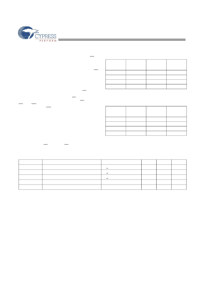
Interleaved Burst Address Table
(MODE = Floating or V
DD
)
First
Address
A1: A0
A1: A0
00
01
10
11
Second
Address
Third
Address
A1: A0
10
11
00
01
Fourth
Address
A1: A0
11
10
01
00
01
00
11
10
Linear Burst Address Table
(MODE = GND)
First
Address
A1: A0
00
01
10
11
Second
Address
A1: A0
01
10
11
00
Third
Address
A1: A0
10
11
00
01
Fourth
Address
A1: A0
11
00
01
10
ZZ Mode Electrical Characteristics
Parameter
Description
Test Conditions
ZZ > V
DD
– 0.2V
ZZ > V
DD
– 0.2V
ZZ < 0.2V
Min
Max
Unit
I
DDZZ
t
ZZS
t
ZZREC
t
ZZI
t
RZZI
Sleep mode standby current
120
mA
Device operation to ZZ
2t
CYC
ns
ZZ recovery time
2t
CYC
ns
ZZ active to sleep current
This parameter is sampled
2t
CYC
ns
ZZ Inactive to exit sleep current
This parameter is sampled
0
ns
相關(guān)PDF資料 |
PDF描述 |
|---|---|
| CY7C1475V25-133BGXI | 72-Mbit (2M x 36/4M x 18/1M x 72) Flow-Through SRAM with NoBL⑩ Architecture |
| CY7C1475V25 | 72-Mbit (2M x 36/4M x 18/1M x 72) Flow-Through SRAM with NoBL Architecture(帶NoBL結(jié)構(gòu)的72-Mbit (2M x 36/4M x 18/1M x 72) Flow-Through SRAM) |
| CY7C1473V25 | 72-Mbit (2M x 36/4M x 18/1M x 72) Flow-Through SRAM with NoBL Architecture(帶NoBL結(jié)構(gòu)的72-Mbit (2M x 36/4M x 18/1M x 72) Flow-Through SRAM) |
| CY7C1475V33 | 72-Mbit (2M x 36/4M x 18/1M x 72) Flow-Through SRAM with NoBL Architecture(帶NoBL結(jié)構(gòu)的72-Mbit (2M x 36/4M x 18/1M x 72) Flow-Through SRAM) |
| CY7C1471V33 | 72-Mbit (2M x 36/4M x 18/1M x 72) Flow-Through SRAM with NoBL Architecture(帶NoBL結(jié)構(gòu)的72-Mbit (2M x 36/4M x 18/1M x 72) Flow-Through SRAM) |
相關(guān)代理商/技術(shù)參數(shù) |
參數(shù)描述 |
|---|---|
| CY7C1475V33-100AXC | 制造商:Cypress Semiconductor 功能描述:72MB (1MBX72) NOBL FLOW-THRU, 3.3V CORE, 2.5/3.3V I/O - Bulk |
| CY7C1475V33-100BGC | 制造商:Cypress Semiconductor 功能描述:SRAM SYNC SGL 3.3V 72MBIT 1MX72 8.5NS 209FBGA - Bulk |
| CY7C1475V33-133BGC | 制造商:Cypress Semiconductor 功能描述:SRAM SYNC OCTAL 3.3V 72MBIT 1MX72 6.5NS 209FBGA - Bulk |
| CY7C14802BC | 制造商:Cypress Semiconductor 功能描述: |
| CY7C14802XC | 制造商:Cypress Semiconductor 功能描述: |
發(fā)布緊急采購(gòu),3分鐘左右您將得到回復(fù)。