- 您現(xiàn)在的位置:買賣IC網(wǎng) > PDF目錄359518 > CY7C138AV-25JC (CYPRESS SEMICONDUCTOR CORP) 3.3V 4K/8K/16K/32K x 8/9 Dual-Port Static RAM PDF資料下載
參數(shù)資料
| 型號(hào): | CY7C138AV-25JC |
| 廠商: | CYPRESS SEMICONDUCTOR CORP |
| 元件分類: | DRAM |
| 英文描述: | 3.3V 4K/8K/16K/32K x 8/9 Dual-Port Static RAM |
| 中文描述: | 4K X 8 DUAL-PORT SRAM, 25 ns, PQCC68 |
| 封裝: | PLASTIC, LCC-68 |
| 文件頁(yè)數(shù): | 7/20頁(yè) |
| 文件大小: | 301K |
| 代理商: | CY7C138AV-25JC |
第1頁(yè)第2頁(yè)第3頁(yè)第4頁(yè)第5頁(yè)第6頁(yè)當(dāng)前第7頁(yè)第8頁(yè)第9頁(yè)第10頁(yè)第11頁(yè)第12頁(yè)第13頁(yè)第14頁(yè)第15頁(yè)第16頁(yè)第17頁(yè)第18頁(yè)第19頁(yè)第20頁(yè)
CY7C138AV/144AV/006AV
CY7C139AV/145AV/016AV
CY7C007AV/017AV
Document #: 38-06051 Rev. *A
Page 7 of 20
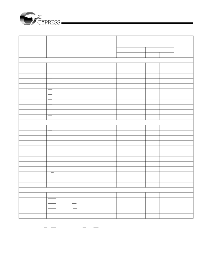
Switching Characteristics
Over the Operating Range
[15]
Parameter
READ CYCLE
t
RC
t
AA
t
OHA
t
ACE[16]
t
DOE
t
LZOE[17, 18, 19]
t
HZOE[17, 18, 19]
t
LZCE[17, 18, 19]
t
HZCE[17, 18, 19]
t
PU[19]
t
PD[19]
WRITE CYCLE
t
WC
t
SCE[16]
t
AW
t
HA
t
SA[16]
t
PWE
t
SD
t
HD
t
HZWE[18, 19]
t
LZWE[18, 19]
t
WDD[20]
t
DDD[20]
BUSY TIMING
[21]
t
BLA
t
BHA
t
BLC
t
BHC
t
PS
Note:
15. Test conditions assume signal transition time of 3 ns or less, timing reference levels of 1.5V, input pulse levels of 0 to 3.0V, and output loading of the specified
I
/I
and 30-pF load capacitance.
16. To access RAM, CE=L, SEM=H. To access semaphore, CE=H and SEM=L. Either condition must be valid for the entire t
SCE
time.
17. At any given temperature and voltage condition for any given device, t
HZCE
is less than t
LZCE
and t
HZOE
is less than t
LZOE
.
18. Test conditions used are Load 3.
19. This parameter is guaranteed but not tested. For information on port-to-port delay through RAM cells from writing port to reading port, refer to Read Timing
with Busy waveform.
20. For information on port-to-port delay through RAM cells from writing port to reading port, refer to Read Timing with Busy waveform.
21. Test conditions used are Load 2.
Description
CY7C138AV/144AV/006AV
CY7C139AV/145AV/016AV
CY7C007AV/017AV
-20
Min.
Max.
Unit
-25
Min.
Max.
Read Cycle Time
Address to Data Valid
Output Hold From Address Change
CE LOW to Data Valid
OE LOW to Data Valid
OE Low to Low Z
OE HIGH to High Z
CE LOW to Low Z
CE HIGH to High Z
CE LOW to Power-Up
CE HIGH to Power-Down
20
25
ns
ns
ns
ns
ns
ns
ns
ns
ns
ns
ns
20
25
3
3
20
12
25
13
3
3
12
15
3
3
12
15
0
0
20
25
Write Cycle Time
CE LOW to Write End
Address Valid to Write End
Address Hold From Write End
Address Set-Up to Write Start
Write Pulse Width
Data Set-Up to Write End
Data Hold From Write End
R/W LOW to High Z
R/W HIGH to Low Z
Write Pulse to Data Delay
Write Data Valid to Read Data Valid
20
16
16
0
0
16
12
0
25
20
20
0
0
20
15
0
ns
ns
ns
ns
ns
ns
ns
ns
ns
ns
ns
ns
12
15
3
3
40
30
50
35
BUSY LOW from Address Match
BUSY HIGH from Address Mismatch
BUSY LOW from CE LOW
BUSY HIGH from CE HIGH
Port Set-Up for Priority
20
20
20
16
20
20
20
17
ns
ns
ns
ns
ns
5
5
相關(guān)PDF資料 |
PDF描述 |
|---|---|
| DR045 | DIGITAL FREQUENCY DISCRIMINATORS |
| DS12887A | Real Time Clock |
| DS1993L-F5 | 1kbit/4kbit Memory iButtonTM DS1994 4-kbit Plus Time Memory iButtonTM |
| DS1922T-F5 | Temperature Logger iButton With 8kB Datalog Memory |
| DS3905U-020 | Triple 128-Position Nonvolatile Digital Variable Resistor/Switch |
相關(guān)代理商/技術(shù)參數(shù) |
參數(shù)描述 |
|---|---|
| CY7C138XC | 制造商:Cypress Semiconductor 功能描述: |
| CY7C139-25JC | 制造商:Cypress Semiconductor 功能描述: |
| CY7C139-25JXC | 功能描述:IC SRAM 36KBIT 25NS 68PLCC RoHS:是 類別:集成電路 (IC) >> 存儲(chǔ)器 系列:- 標(biāo)準(zhǔn)包裝:1,000 系列:- 格式 - 存儲(chǔ)器:RAM 存儲(chǔ)器類型:移動(dòng) SDRAM 存儲(chǔ)容量:256M(8Mx32) 速度:133MHz 接口:并聯(lián) 電源電壓:1.7 V ~ 1.95 V 工作溫度:-40°C ~ 85°C 封裝/外殼:90-VFBGA 供應(yīng)商設(shè)備封裝:90-VFBGA(8x13) 包裝:帶卷 (TR) 其它名稱:557-1327-2 |
| CY7C1392CV18-200BZC | 功能描述:靜態(tài)隨機(jī)存取存儲(chǔ)器 2Mx8 1.8V DDR II SIO 靜態(tài)隨機(jī)存取存儲(chǔ)器 RoHS:否 制造商:Cypress Semiconductor 存儲(chǔ)容量:16 Mbit 組織:1 M x 16 訪問時(shí)間:55 ns 電源電壓-最大:3.6 V 電源電壓-最小:2.2 V 最大工作電流:22 uA 最大工作溫度:+ 85 C 最小工作溫度:- 40 C 安裝風(fēng)格:SMD/SMT 封裝 / 箱體:TSOP-48 封裝:Tray |
| CY7C1392CV18-250BZC | 功能描述:靜態(tài)隨機(jī)存取存儲(chǔ)器 2Mx8 1.8V DDR II SIO 靜態(tài)隨機(jī)存取存儲(chǔ)器 RoHS:否 制造商:Cypress Semiconductor 存儲(chǔ)容量:16 Mbit 組織:1 M x 16 訪問時(shí)間:55 ns 電源電壓-最大:3.6 V 電源電壓-最小:2.2 V 最大工作電流:22 uA 最大工作溫度:+ 85 C 最小工作溫度:- 40 C 安裝風(fēng)格:SMD/SMT 封裝 / 箱體:TSOP-48 封裝:Tray |
發(fā)布緊急采購(gòu),3分鐘左右您將得到回復(fù)。