- 您現(xiàn)在的位置:買賣IC網(wǎng) > PDF目錄379058 > CY7C1256V18-300BZXC (CYPRESS SEMICONDUCTOR CORP) 36-Mbit QDR⑩-II+ SRAM 4-Word Burst Architecture (2.0 Cycle Read Latency) PDF資料下載
參數(shù)資料
| 型號: | CY7C1256V18-300BZXC |
| 廠商: | CYPRESS SEMICONDUCTOR CORP |
| 元件分類: | DRAM |
| 英文描述: | 36-Mbit QDR⑩-II+ SRAM 4-Word Burst Architecture (2.0 Cycle Read Latency) |
| 中文描述: | 4M X 9 QDR SRAM, 0.45 ns, PBGA165 |
| 封裝: | 15 X 17 MM, 1.40 MM HEIGHT, LEAD FREE, MO-216, FBGA-165 |
| 文件頁數(shù): | 18/28頁 |
| 文件大?。?/td> | 1042K |
| 代理商: | CY7C1256V18-300BZXC |
第1頁第2頁第3頁第4頁第5頁第6頁第7頁第8頁第9頁第10頁第11頁第12頁第13頁第14頁第15頁第16頁第17頁當(dāng)前第18頁第19頁第20頁第21頁第22頁第23頁第24頁第25頁第26頁第27頁第28頁
CY7C1241V18
CY7C1256V18
CY7C1243V18
CY7C1245V18
Document Number: 001-06365 Rev. *C
Page 18 of 28
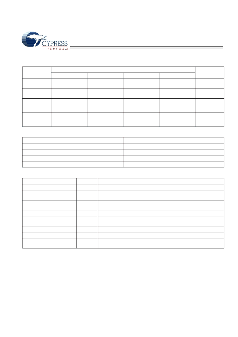
Identification Register Definitions
Instruction
Field
Value
Description
CY7C1241V18
CY7C1256V18
CY7C1243V18
CY7C1245V18
Revision
Number (31:29)
000
000
000
000
Version number.
Cypress Device
ID (28:12)
11010010101000111 11010010101001111 11010010101010111 11010010101100111 Defines the type
of SRAM.
Cypress JEDEC
ID (11:1)
00000110100
00000110100
00000110100
00000110100
Enables unique
identification of
SRAM vendor.
ID Register
Presence (0)
1
1
1
1
Indicates the
presence of an
ID register.
Scan Register Sizes
Register Name
Bit Size
Instruction
3
Bypass
1
ID
32
Boundary Scan
109
Instruction Codes
Instruction
Code
Description
EXTEST
000
Captures the input/output ring contents.
IDCODE
001
Loads the ID register with the vendor ID code and places the register between
TDI and TDO. This operation does not affect SRAM operation.
SAMPLE Z
010
Captures the input/output contents. Places the boundary scan register between
TDI and TDO. Forces all SRAM output drivers to a High-Z state.
RESERVED
011
Do Not Use: This instruction is reserved for future use.
SAMPLE/PRELOAD
100
Captures the input/output ring contents. Places the boundary scan register
between TDI and TDO. Does not affect the SRAM operation.
RESERVED
101
Do Not Use: This instruction is reserved for future use.
RESERVED
110
Do Not Use: This instruction is reserved for future use.
BYPASS
111
Places the bypass register between TDI and TDO. This operation does not affect
SRAM operation.
[+] Feedback
相關(guān)PDF資料 |
PDF描述 |
|---|---|
| CY7C1256V18-300BZXI | 36-Mbit QDR⑩-II+ SRAM 4-Word Burst Architecture (2.0 Cycle Read Latency) |
| CY7C1246V18 | 36-Mbit DDR-II+ SRAM 2-Word Burst Architecture (2.0 Cycle Read Latency) |
| CY7C1250V18-300BZXI | 36-Mbit DDR-II+ SRAM 2-Word Burst Architecture (2.0 Cycle Read Latency) |
| CY7C1250V18-333BZC | 36-Mbit DDR-II+ SRAM 2-Word Burst Architecture (2.0 Cycle Read Latency) |
| CY7C1250V18-333BZI | 36-Mbit DDR-II+ SRAM 2-Word Burst Architecture (2.0 Cycle Read Latency) |
相關(guān)代理商/技術(shù)參數(shù) |
參數(shù)描述 |
|---|---|
| CY7C1262XV18-366BZXC | 功能描述:靜態(tài)隨機(jī)存取存儲器 36MB (2Mx18) 1.8v 366MHz QDR II 靜態(tài)隨機(jī)存取存儲器 RoHS:否 制造商:Cypress Semiconductor 存儲容量:16 Mbit 組織:1 M x 16 訪問時(shí)間:55 ns 電源電壓-最大:3.6 V 電源電壓-最小:2.2 V 最大工作電流:22 uA 最大工作溫度:+ 85 C 最小工作溫度:- 40 C 安裝風(fēng)格:SMD/SMT 封裝 / 箱體:TSOP-48 封裝:Tray |
| CY7C1262XV18-450BZXC | 功能描述:靜態(tài)隨機(jī)存取存儲器 36MB (2Mx18) 1.8v 450MHz QDR II 靜態(tài)隨機(jī)存取存儲器 RoHS:否 制造商:Cypress Semiconductor 存儲容量:16 Mbit 組織:1 M x 16 訪問時(shí)間:55 ns 電源電壓-最大:3.6 V 電源電壓-最小:2.2 V 最大工作電流:22 uA 最大工作溫度:+ 85 C 最小工作溫度:- 40 C 安裝風(fēng)格:SMD/SMT 封裝 / 箱體:TSOP-48 封裝:Tray |
| CY7C12631KV18-400BZI | 功能描述:靜態(tài)隨機(jī)存取存儲器 2Mb X 18 400MHz QDR-II+ 靜態(tài)隨機(jī)存取存儲器 RoHS:否 制造商:Cypress Semiconductor 存儲容量:16 Mbit 組織:1 M x 16 訪問時(shí)間:55 ns 電源電壓-最大:3.6 V 電源電壓-最小:2.2 V 最大工作電流:22 uA 最大工作溫度:+ 85 C 最小工作溫度:- 40 C 安裝風(fēng)格:SMD/SMT 封裝 / 箱體:TSOP-48 封裝:Tray |
| CY7C1263KV18-400BZC | 功能描述:靜態(tài)隨機(jī)存取存儲器 36MB (2Mx18) 1.8v 400MHz QDR II 靜態(tài)隨機(jī)存取存儲器 RoHS:否 制造商:Cypress Semiconductor 存儲容量:16 Mbit 組織:1 M x 16 訪問時(shí)間:55 ns 電源電壓-最大:3.6 V 電源電壓-最小:2.2 V 最大工作電流:22 uA 最大工作溫度:+ 85 C 最小工作溫度:- 40 C 安裝風(fēng)格:SMD/SMT 封裝 / 箱體:TSOP-48 封裝:Tray |
| CY7C1263KV18-400BZI | 功能描述:靜態(tài)隨機(jī)存取存儲器 36MB (2Mx18) 1.8v 400MHz QDR II 靜態(tài)隨機(jī)存取存儲器 RoHS:否 制造商:Cypress Semiconductor 存儲容量:16 Mbit 組織:1 M x 16 訪問時(shí)間:55 ns 電源電壓-最大:3.6 V 電源電壓-最小:2.2 V 最大工作電流:22 uA 最大工作溫度:+ 85 C 最小工作溫度:- 40 C 安裝風(fēng)格:SMD/SMT 封裝 / 箱體:TSOP-48 封裝:Tray |
發(fā)布緊急采購,3分鐘左右您將得到回復(fù)。