- 您現(xiàn)在的位置:買(mǎi)賣IC網(wǎng) > PDF目錄384268 > CY2PP3220 Clocks and Buffers PDF資料下載
參數(shù)資料
| 型號(hào): | CY2PP3220 |
| 英文描述: | Clocks and Buffers |
| 中文描述: | 時(shí)鐘和緩沖器 |
| 文件頁(yè)數(shù): | 4/12頁(yè) |
| 文件大?。?/td> | 246K |
| 代理商: | CY2PP3220 |
PRELIMINARY
FastEdge Series
CY2PP3115
Document #: 38-07502 Rev.*A
Page 4 of 12
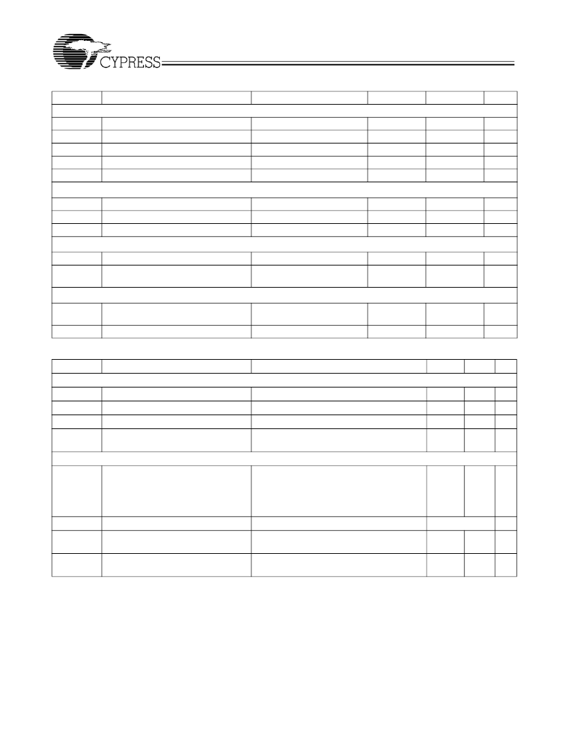
ECL DC Electrical Specifications
Parameter
Control (FSEL(A,B,C),CLK_SEL, MR and FSELD) (ECL single-ended)
V
EE2.5
–2.5 Negative Power Supply
V
EE3.3
–3.3 Negative Power Supply
V
IL
Input Voltage, Low
V
IH
Input Voltage, High
I
IN
Description
Condition
Min.
Max.
Unit
–2.5V ± 5%, V
EE
= 0.0V
–3.3V ± 5%, V
EE
= 0.0V
–2.375
–33.135
–1.945
–1.165
–2.625
–3.465
–1.625
–0.880
I150I
V
V
V
V
uA
Input Current
[10]
V
IN
= V
IL
or V
IN
= V
IH
Clock input pair CLK0,
CLK0#,CLK1,CLK1# (ECL differential signals)
V
PP
V
CMR
I
IN
Differential input voltage
[11]
Differential cross point voltage
[12]
Input Current
[10]
Differential operation
Differential operation
V
IN
= V
IL
or V
IN
= V
IH
0.1
1.3
–0.5
I150I
V
V
uA
V
EE
+1.2
ECL Outputs QA((0:1),#),QB((0:2),
#
),QC((0:3),
#
),QD((0:5),
#
)(ECL differential signals)
V
OH
Output High Voltage
V
OL
Output Low Voltage
V
EE
= –3.3V ± 5%,V
EE
= –2.5V ± 5%
I
OH
= –30 mA
[13]
I
OL
= –5 ma
[13]
–1.2
–1.945
–1.945
–0.7
–1.5
–1.3
V
V
Supply current and VBB
I
EE
Maximum Quiescent Supply Current
without output termination current
[14]
Output reference voltage
V
EE
pin
–
180
mA
V
BB
I
BB
= 200 uA
–1.620
–1.220
V
AC Electrical Specifications
Parameter
Description
Condition
Min.
Max.
Unit
Clock input pair CLK0,
CLK0#,CLK1,CLK1#(PECL or ECL differential signals)
Differential input voltage
[16]
Differential cross point voltage
[17]
Input Frequency
[18]
V
PP
V
CMR
F
CLK
T
PD
Differential operation
0.1
1.3
V
Differential operation
V
EE
+ 1.2
0
V
50% duty cycle Standard load
1500
MHz
Propagation Delay CLK0 or CLK1 to
QA(0:1),QB(0:2),QC(0:3),QD(0:5)
pair
660 MHz 50% duty cycle Standard load Differ-
ential Operation. See
Table 2
600
1200
ps
ECL/PECL Clock Outputs QA((0:1),#),QB((0:2),
#
),QC((0:3),
#
),QD((0:5),
#
) (differential)
Vo
(P-P)
Differential output voltage
(peak-to-peak)
Differential PRBS
fo < 50 MHz
fo < 0.8 GHz
fo < 1.0 GHz
fo < 1.5 GHz
0.45
0.4
0.375
0.3
V
VMCR
Common Voltage Range
V
CC
–1.425
–
ps
tsk
(O)
Output-to-output skew
660 MHz 50% duty cycle Standard load Differ-
ential Operation
50
ps
tsk
(O)
Output-to-output skew (different
frequency)
660 MHz 50% duty cycle Standard load Differ-
ential Operation
–
60
ps
Notes:
10. Input have internal pullup / pulldown or biasing resistors which affect the input current.
11.
VPP (DC) is the minimum differential input voltage swing required to maintain device functionality.
12. VCMR (DC) is the crosspoint of the differential input signal. Functional operation is obtained when the crosspoint is within the VCMR (DC) range and the input
swing lies within the VPP (DC) specification.
13. Equivalent to a termination of 50
to VTT.
14. I
CC
Calculation: ICC = (number of differential output pairs used) x (I
OH
+ I
OL
) + IEE or I
CC
= (number of differential output pairs used) x (V
OH
–VTT)/Rload +
(V
OL
–VTT)/Rload +I
EE
.
15. AC characteristics apply for parallel output termination of 50
to VTT.
16. VPP (AC) is the minimum differential ECL/PECL input swing required to maintain AC characteristics including tpd and device-to-device skew.
17. VCMR (AC) is the crosspoint of the differential ECL/PECL input signal. Normal AC operation is obtained when the crosspoint is within the VCMR(AC) range and
the input swing lies within the VPP(AC) specification. Violation of VCMR(AC) or VPP(AC) impacts the device propagation delay, device and part-to-part skew.
18. The CY2PP3115 is fully operation up to 1.5 GHz.
相關(guān)PDF資料 |
PDF描述 |
|---|---|
| CY2PP326 | Clocks and Buffers |
| CZT2222 | NPN SILICON TRANSISTOR |
| CZT2222A | NPN SILICON TRANSISTOR |
| CZT3904NPN | MC680X0 FPU COPROCESSOR |
| CZT3904 | COMPLEMENTARY SILICON TRANSISTORS |
相關(guān)代理商/技術(shù)參數(shù) |
參數(shù)描述 |
|---|---|
| CY2PP3220AI | 功能描述:時(shí)鐘緩沖器 2.5V or 3.3V 1.5GHz IND RoHS:否 制造商:Texas Instruments 輸出端數(shù)量:5 最大輸入頻率:40 MHz 傳播延遲(最大值): 電源電壓-最大:3.45 V 電源電壓-最小:2.375 V 最大功率耗散: 最大工作溫度:+ 85 C 最小工作溫度:- 40 C 封裝 / 箱體:LLP-24 封裝:Reel |
| CY2PP3220AIT | 制造商:CYPRESS 制造商全稱:Cypress Semiconductor 功能描述:Dual 1:10 Differential Clock / Data Fanout Buffer |
| CY2PP326 | 制造商:CYPRESS 制造商全稱:Cypress Semiconductor 功能描述:2 x 2 Clock and Data Switch Buffer |
| CY2PP326AI | 功能描述:時(shí)鐘驅(qū)動(dòng)器及分配 2.5V or 3.3V 1.5GHz IND RoHS:否 制造商:Micrel 乘法/除法因子:1:4 輸出類型:Differential 最大輸出頻率:4.2 GHz 電源電壓-最大: 電源電壓-最小:5 V 最大工作溫度:+ 85 C 封裝 / 箱體:SOIC-8 封裝:Reel |
| CY2PP326AIT | 制造商:CYPRESS 制造商全稱:Cypress Semiconductor 功能描述:2 x 2 Clock and Data Switch Buffer |
發(fā)布緊急采購(gòu),3分鐘左右您將得到回復(fù)。