- 您現(xiàn)在的位置:買賣IC網(wǎng) > PDF目錄384268 > CY2PP3220 Clocks and Buffers PDF資料下載
參數(shù)資料
| 型號: | CY2PP3220 |
| 英文描述: | Clocks and Buffers |
| 中文描述: | 時鐘和緩沖器 |
| 文件頁數(shù): | 2/12頁 |
| 文件大?。?/td> | 246K |
| 代理商: | CY2PP3220 |
PRELIMINARY
FastEdge Series
CY2PP3115
Document #: 38-07502 Rev.*A
Page 2 of 12
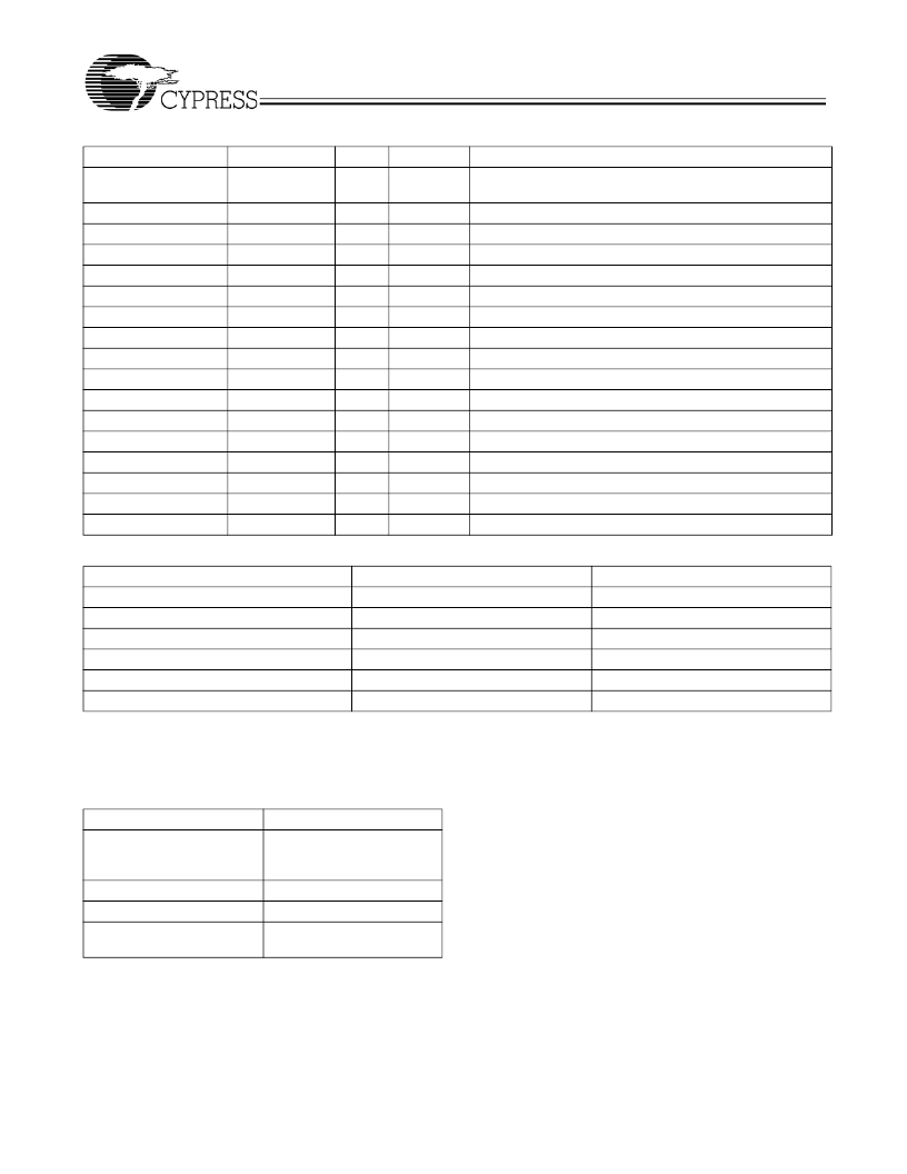
Pin Description
Governing Agencies
The following agencies provide specifications that apply to the
CY2PP3115. The agency name and relevant specification is
listed below.
Pin No.
Name
[2,3]
VCC
I/O
[1]
+PWR
Type
Description
1,14,27, 30, 39, 40, 47,
52
2
3,4,11,12
5,8
6,9
10
13
28,29
7
26,24,22,20,18,16
25,23,21,19,17,15
38,36,34,32
37,35,33,31
46,44,42
45,43,41
51,49
50,48
POWER
Power Supply, positive connection
MR
FSEL(A,B,C,D)
CLK(0:1)
CLK(0:1)#
VBB
VEE
NC
CLK_SEL
QD(0:5)
QD(0:5)#
QC(0:3)
QC(0:3)#
QB(0:2)
QB(0:2)#
QA(0:1)
QA(0:1)#
I,PD
I,PD
I,PD
I,PC
O
–PWR
ECL/PECL
ECL/PECL
ECL/PECL
ECL/PECL
Bias
POWER
Reset
Output Divider Selects
Differential Clock Inputs – TRUE
Differential Clock Inputs – COMPLIMENT
DC Bias Source
Power Supply, Negative Connection
No Connect. Pad Only
Clock Input Select
Bank D True Output
Bank D Compliment Output
Bank C True Output
Bank C Compliment Output
Bank B True Output
Bank B Compliment Output
Bank A True Output
Bank A Compliment Output
I,PD
O,OE
O,OE
O,OE
O,OE
O,OE
O,OE
O,OE
O,OE
ECL/PECL
ECL/PECL
ECL/PECL
ECL/PECL
ECL/PECL
ECL/PECL
ECL/PECL
ECL/PECL
ECL/PECL
Table 1. Function Table
Control Pin
0
÷1
÷1
÷1
÷1
1
÷2
÷2
÷2
÷2
FSELA (Asynchronous)
FSELB (Asynchronous)
FSELC (Asynchronous)
FSELD (Asynchronous)
CLK_SEL (Asynchronous)
MR (Asynchronous)
CLK0
Active
CLK1
Reset (QX = L and QX# = H)
Agency Name
JEDEC
Specification
JESD 51 (Theta JA)
JESD 8–2 (ECL)
JESD 65–A (skew,jitter)
1596.3 (Jitter specs)
94 (Flammability Grading)
883E Method 1012.1
(Thermal Theta JC)
IEEE
UL
Mil–Spec
Notes:
1.
In the I/O column, the following notation is used: I for Input, O for Output, PD for Pull-down, PU for Pull-up, PC for Pull Center, O for output, OE for open emitter
and PWR for Power.
In ECL mode (negative power supply mode), V
is either –3.3V or –2.5V and V
is connected to GND (0V). In PECL mode (positive power supply mode),
V
is connected to GND (0V) and V
CC
is either +3.3V or +2.5V. In both modes, the input and output levels are referenced to the most positive supply (V
CC
)
and are between VCC and VEE.
V
BB
is available for use for single ended bias mode when V
CC
is +3.3V.
2.
3.
相關PDF資料 |
PDF描述 |
|---|---|
| CY2PP326 | Clocks and Buffers |
| CZT2222 | NPN SILICON TRANSISTOR |
| CZT2222A | NPN SILICON TRANSISTOR |
| CZT3904NPN | MC680X0 FPU COPROCESSOR |
| CZT3904 | COMPLEMENTARY SILICON TRANSISTORS |
相關代理商/技術參數(shù) |
參數(shù)描述 |
|---|---|
| CY2PP3220AI | 功能描述:時鐘緩沖器 2.5V or 3.3V 1.5GHz IND RoHS:否 制造商:Texas Instruments 輸出端數(shù)量:5 最大輸入頻率:40 MHz 傳播延遲(最大值): 電源電壓-最大:3.45 V 電源電壓-最小:2.375 V 最大功率耗散: 最大工作溫度:+ 85 C 最小工作溫度:- 40 C 封裝 / 箱體:LLP-24 封裝:Reel |
| CY2PP3220AIT | 制造商:CYPRESS 制造商全稱:Cypress Semiconductor 功能描述:Dual 1:10 Differential Clock / Data Fanout Buffer |
| CY2PP326 | 制造商:CYPRESS 制造商全稱:Cypress Semiconductor 功能描述:2 x 2 Clock and Data Switch Buffer |
| CY2PP326AI | 功能描述:時鐘驅動器及分配 2.5V or 3.3V 1.5GHz IND RoHS:否 制造商:Micrel 乘法/除法因子:1:4 輸出類型:Differential 最大輸出頻率:4.2 GHz 電源電壓-最大: 電源電壓-最小:5 V 最大工作溫度:+ 85 C 封裝 / 箱體:SOIC-8 封裝:Reel |
| CY2PP326AIT | 制造商:CYPRESS 制造商全稱:Cypress Semiconductor 功能描述:2 x 2 Clock and Data Switch Buffer |
發(fā)布緊急采購,3分鐘左右您將得到回復。