- 您現(xiàn)在的位置:買賣IC網(wǎng) > PDF目錄379008 > CY2DP814ZCT (CYPRESS SEMICONDUCTOR CORP) DB37 INTERFACE DATA CBL DB37 Male - DB37 Female PDF資料下載
參數(shù)資料
| 型號(hào): | CY2DP814ZCT |
| 廠商: | CYPRESS SEMICONDUCTOR CORP |
| 元件分類: | 時(shí)鐘及定時(shí) |
| 英文描述: | DB37 INTERFACE DATA CBL DB37 Male - DB37 Female |
| 中文描述: | 2DP SERIES, LOW SKEW CLOCK DRIVER, 4 TRUE OUTPUT(S), 0 INVERTED OUTPUT(S), PDSO16 |
| 封裝: | 4.40 MM, MO-153, PLASTIC, TSSOP-16 |
| 文件頁數(shù): | 4/9頁 |
| 文件大小: | 120K |
| 代理商: | CY2DP814ZCT |
ComLink
Series
CY2DP814
Document #: 38-07060 Rev. *B
Page 4 of 9
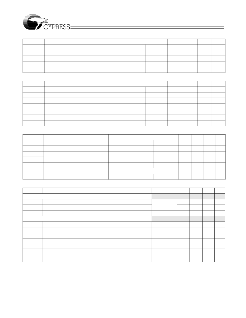
Table 6. D.C. Electrical Characteristics: 3.3V
–
LVPECL Input
Parameter
I
V
ID
I
VCM
I
IH
I
IL
I
I
Description
Condition
Min.
400
1650
Typ.
Max.
2600
2250
±20
±20
±20
Unit
mV
mV
uA
uA
uA
Differential Input Voltage p-p
Common-mode Voltage
Input High Current
Input Low Current
Input High Current
Guaranteed Logic High Level
V
DD
= Max.
V
DD
= Max.
V
DD
= Max.,
V
IN
=
V
DD
(max.)
V
IN
= V
DD
V
IN
= V
SS
±10
±10
Table 7. D.C Electrical Characteristics: 3.3V
–
LVTTL/LVCMOS Input
Parameter
V
IH
V
IL
I
IH
I
IL
I
I
V
IK
V
H
Description
Condition
Min.
2
Typ.
Max.
Unit
V
V
uA
uA
uA
V
mV
Input High Voltage
Input Low Voltage
Input High Current
Input Low Current
Input High Current
Clamp Diode Voltage
Input Hysteresis
Guaranteed Logic High Level
Guaranteed Logic Low Level
V
DD
= Max.
V
DD
= Max.
V
DD
= Max.,
V
IN
=
V
DD
(max.)
V
DD
= Min.,
I
IN
=
–
18 mA
0.8
1
–
1
20
–
1.2
V
IN
= 2.7V
V
IN
= 0.5V
–
0.7
80
Table 8. D.C Electrical Characteristics: 3.3V
–
LVPECL Output
Parameter
I
V
OD
I
I
V
OC
I
Rise Time
Fall Time
V
OH
V
OL
I
OS
Description
Condition
Min.
1000
Typ.
Max.
3600
226
Unit
mV
mV
Driver Differential Output Voltage p-p
Driver common-mode p-p
V
DD
= Min.,
V
IN
=
V
IH
or
V
IL
V
DD
= Min.,
V
IN
=
V
IH
or
V
IL
RL = 50 ohm
RL = 50 ohm
RL = 50 ohm
Differential 20% to 80%
CL
–
10 pF RL and CL to
G
ND
300
800
pS
Output High Voltage
Output Low Voltage
Short Circuit Current
V
DD
= Min.,
V
IN
=
V
IH
or
V
IL
User-defined (see
Figure 1
)
V
DD
= Max.,
V
OUT
=
G
ND
I
OH
=
–
12 mA
2.1
3.0
V
V
–
125
–
150
mA
Table 9. AC Switching Characteristics @ 3.3V
V
DD
= 3.3V ±5%, Temperature =
–
40
°
C to +85
°
C
Parameter
Description
IN [+,-] to Q[A,B] Data & Clock Speed
t
PLH
Propagation Delay
–
Low to High
t
PHL
Propagation Delay
–
High to Low
t
PD
Propagation Delay
EN [1,2] to Q[A,B] Control Speed
t
PE
Enable (EN) to functional operation
Tpd
Functional operation to Disable
t
SK(0)
Output Skew: Skew between outputs of the same package (in phase)
Pulse Skew: Skew between opposite transitions of the same output
(t
PHL
–
t
PLH
)
Package Skew: Skew between outputs of different packages at the
same power supply voltage, temperature and package type. Same
input signal level and output load.
Conditions
Min.
Typ.
Max.
Unit
V
OD
= 100 mV
3
3
3
4
4
4
5
5
5
nS
nS
ns
6
5
nS
nS
nS
nS
0.2
t
SK(p)
0.2
t
SK(t)
V
ID
= 100 mV
1
nS
相關(guān)PDF資料 |
PDF描述 |
|---|---|
| CY2DP814 | 1:4 Clock Fanout Buffer |
| CY2DP814SCT | 1:4 Clock Fanout Buffer |
| CY2DP814SI | 1:4 Clock Fanout Buffer |
| CY2DP814SIT | 1:4 Clock Fanout Buffer |
| CY2DP814ZI | 1:4 Clock Fanout Buffer |
相關(guān)代理商/技術(shù)參數(shù) |
參數(shù)描述 |
|---|---|
| CY2DP814ZI | 制造商:CYPRESS 制造商全稱:Cypress Semiconductor 功能描述:1:4 Clock Fanout Buffer |
| CY2DP814ZIT | 制造商:CYPRESS 制造商全稱:Cypress Semiconductor 功能描述:1:4 Clock Fanout Buffer |
| CY2DP814ZXC | 功能描述:時(shí)鐘緩沖器 3.3V 400MHz LVDS Buffer RoHS:否 制造商:Texas Instruments 輸出端數(shù)量:5 最大輸入頻率:40 MHz 傳播延遲(最大值): 電源電壓-最大:3.45 V 電源電壓-最小:2.375 V 最大功率耗散: 最大工作溫度:+ 85 C 最小工作溫度:- 40 C 封裝 / 箱體:LLP-24 封裝:Reel |
| CY2DP814ZXCT | 功能描述:時(shí)鐘緩沖器 3.3V 450MHz COM RoHS:否 制造商:Texas Instruments 輸出端數(shù)量:5 最大輸入頻率:40 MHz 傳播延遲(最大值): 電源電壓-最大:3.45 V 電源電壓-最小:2.375 V 最大功率耗散: 最大工作溫度:+ 85 C 最小工作溫度:- 40 C 封裝 / 箱體:LLP-24 封裝:Reel |
| CY2DP814ZXI | 功能描述:時(shí)鐘緩沖器 3.3V 450MHz IND RoHS:否 制造商:Texas Instruments 輸出端數(shù)量:5 最大輸入頻率:40 MHz 傳播延遲(最大值): 電源電壓-最大:3.45 V 電源電壓-最小:2.375 V 最大功率耗散: 最大工作溫度:+ 85 C 最小工作溫度:- 40 C 封裝 / 箱體:LLP-24 封裝:Reel |
發(fā)布緊急采購,3分鐘左右您將得到回復(fù)。