- 您現(xiàn)在的位置:買賣IC網(wǎng) > PDF目錄379006 > CY28341OC (CYPRESS SEMICONDUCTOR CORP) Universal Single-Chip Clock Solution for VIA P4M266/KM266 DDR Systems PDF資料下載
參數(shù)資料
| 型號(hào): | CY28341OC |
| 廠商: | CYPRESS SEMICONDUCTOR CORP |
| 元件分類: | XO, clock |
| 英文描述: | Universal Single-Chip Clock Solution for VIA P4M266/KM266 DDR Systems |
| 中文描述: | 200 MHz, PROC SPECIFIC CLOCK GENERATOR, PDSO56 |
| 封裝: | SSOP-56 |
| 文件頁(yè)數(shù): | 3/21頁(yè) |
| 文件大?。?/td> | 189K |
| 代理商: | CY28341OC |
第1頁(yè)第2頁(yè)當(dāng)前第3頁(yè)第4頁(yè)第5頁(yè)第6頁(yè)第7頁(yè)第8頁(yè)第9頁(yè)第10頁(yè)第11頁(yè)第12頁(yè)第13頁(yè)第14頁(yè)第15頁(yè)第16頁(yè)第17頁(yè)第18頁(yè)第19頁(yè)第20頁(yè)第21頁(yè)
CY28341
Document #: 38-07367 Rev. *A
Page 3 of 21
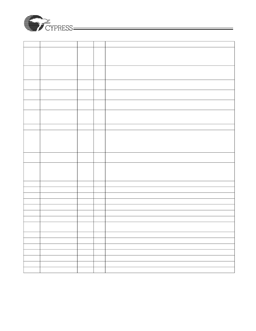
Note:
2.
PU = internal Pull-up. PD = internal Pull-down. Typically = 250 kW (range 200 kW to 500 kW).
11
SELSDR_DDR#/PCI
1
VDDPCI
I/O
PD
Power-on Bidirectional Input/Output
. At power-up, SELSDR_DDR is the
input. When the power supply voltage crosses the input threshold voltage,
SELSDR_DDR state is latched and this pin becomes PCI clock
output.SelSDR_DDR#. = 0, DDR Mode. SelSDR_DDR#. = 1, SDR Mode.
Power-on Bidirectional Input/Output
. At power-up, FS2 is the input. When
the power supply voltage crosses the input threshold voltage, FS2 state is
latched and this pin becomes 24_48M, a SIO programmable clock output.
AGP Clock Output
. Is synchronous to CPU clocks. See
Table 1
.
21
FS2/24_48M
VDD48M
I/O
PD
6
AGP0
VDDAG
P
VDDAG
P
O
8
AGP2
O
AGP Clock Output
. Is synchronous to CPU clocks. See
Table 1
.
25
IREF
I
Current reference programming input for CPU buffers. A precise resistor is
attached to this pin, which is connected to the internal current reference.
Serial Data Input
. Conforms to the Philips I2C specification of a Slave
Receive/Transmit device. It is an input when receiving data. It is an open drain
output when acknowledging or transmitting data.
Serial Clock Input
. Conforms to the Philips I2C specification.
Power-down Input/System Reset Control Output
. If Byte6 Bit7 = 0, this pin
becomes a SRESET# open drain output, and the internal pulled up is not active.
See system reset description. If Byte6 Bit7 = 1 (default), this pin becomes PD#
input with an internal pull-up. When PD# is asserted LOW, the device enters
power-down mode. See power management function.
If SelSDR_DDR#.= 0, 2.5V CMOS type input to the DDR differential buffers.If
SelSDR_DDR#.= 1, 3.3V CMOS type input to the SDR buffer.
If SelSDR_DDR#.= 0, 2.5V single ended SDRAM buffered output of the signal
applied at BUF_IN. It is in phase with the DDRT(0:5) signals.If
SelSDR_DDR#.= 1, 3.3V single ended SDRAM buffered output of the signal
applied at BUF_IN. It is in phase with the SDRAM(0:11) signals
3.3V Power Supply for AGP clocks
3.3V Power Supply for CPUT/C clocks
3.3V Power Supply for PCI clocks
3.3V Power Supply for REF clock
2.5V Power Supply for CPUCS_T/C clocks
3.3V Power Supply for 48M
3.3V Common Power Supply
If SelSDR_DDR#.= 0, 2.5V Power Supply for DDR clocksIf SelSDR_DDR#.=
1, 3.3V Power Supply for SDR clocks.
Ground for AGP clocks
Ground for PCI clocks
Ground for CPUT/C clocks
Ground for DDR clocks
Ground for 48M clock
Ground for ICPUCS_T/C clocks
Common Ground
28
SDATA
I/O
27
26
SCLK
PD#/SRESET#
I
I/O
PU
45
BUF_IN
46
FBOUT
5
51
16
55
50
22
23
34,40
VDDAGP
VDDC
VDDPCI
VDDR
VDDI
VDD48M
VDD
VDDD
9
13
54
33,39
19
47
24
VSSAGP
VSSPCI
VSSC
VSSD
VSS48M
VSSI
VSS
Pin Description
[2]
(continued)
Pin
Name
PWR
I/O
Description
相關(guān)PDF資料 |
PDF描述 |
|---|---|
| CY28346 | Clock Synthesizer with Differential CPU Outputs |
| CY28346OC | CONN BNC PLUG CRIMP RG-TFE-59,62 |
| CY28346OCT | CONN BNC PLUG CRIMP RG-59,62 |
| CY28346ZC | Clock Synthesizer with Differential CPU Outputs |
| CY28346ZCT | Clock Synthesizer with Differential CPU Outputs |
相關(guān)代理商/技術(shù)參數(shù) |
參數(shù)描述 |
|---|---|
| CY28341OC-2 | 制造商:Rochester Electronics LLC 功能描述:- Bulk |
| CY28341OC-2T | 制造商:CYPRESS 制造商全稱:Cypress Semiconductor 功能描述:Universal Clock Chip for VIA⑩P4M/KT/KM400 DDR Systems |
| CY28341OC-3 | 制造商:CYPRESS 制造商全稱:Cypress Semiconductor 功能描述:Universal Clock Chip for VIA⑩P4M/KT/KM400A DDR Systems |
| CY28341OC-3T | 制造商:Rochester Electronics LLC 功能描述:- Tape and Reel |
| CY28341OCT | 制造商:SPECTRALINEAR 制造商全稱:SPECTRALINEAR 功能描述:Universal Single-Chip Clock Solution for VIA P4M266/KM266 DDR Systems |
發(fā)布緊急采購(gòu),3分鐘左右您將得到回復(fù)。