- 您現(xiàn)在的位置:買賣IC網(wǎng) > PDF目錄379002 > CY25200 (Cypress Semiconductor Corp.) Programmable Spread Spectrum Clock Generator for EMI Reduction PDF資料下載
參數(shù)資料
| 型號: | CY25200 |
| 廠商: | Cypress Semiconductor Corp. |
| 英文描述: | Programmable Spread Spectrum Clock Generator for EMI Reduction |
| 中文描述: | 可編程擴頻時鐘發(fā)生器減少電磁干擾 |
| 文件頁數(shù): | 3/11頁 |
| 文件大小: | 280K |
| 代理商: | CY25200 |
CY25200
Document #: 38-07633 Rev. *A
Page 3 of 11
Programming Description
Customers planning to use the CY25200 need to provide the
programming information described as “ENTER DATA” in
Table 1
and Table 2,
then
should contact local Cypress Sales.
Additional information on the CY25200 can be obtained from
the Cypress web site at www.cypress.com.
Product Functions
Control Pins (CP0, CP1, CP2 and CP3)
There are four control signals available through programming
of pins 4, 10, 14 and 15.
CP0 (pin 4) and CP1 (pin10) are specifically designed to
function
as
control
pins.
(SSCLK5/REFOUT/CP2) and 15 (SSCLK6/REFOUT/CP3)
are multi-functional and can be programmed to be a control
signal or an output clock (SSCLK or REFOUT). All of the
control pins, CP0, CP1, CP2 and CP3 are programmable and
can be programmed to have only one of the following
functions:
However
pins
14
Output Enable (OE), if OE = 1, all the SSCLK or REFOUT
outputs are enabled
SSON, Spread spectrum control, 1 = spread on and 0 =
spread off
CLKSEL, SSCLK output frequency select
PD#, Active Low, PD# = 0, all the outputs are three-stated
and the part enters a low-power state
The last control signal is the Power down (PD#) that can be
implemented only through programming CP0 or CP1 (CP2
and CP3 can not be programmed as PD#). Here is an ex-
ample with 3 control pins,
CLKIN = 33MHz
SSCLK1/2/3/4 = 100MHz with ±1% Spread
SSCLK 5 = REFOUT(33MHz)
CP0 (Pin 4) = PD#
CP1 (Pin 10) = OE
CP3 (pin 15) = SSON
The pinout for the above example is shown in
Figure 1
.
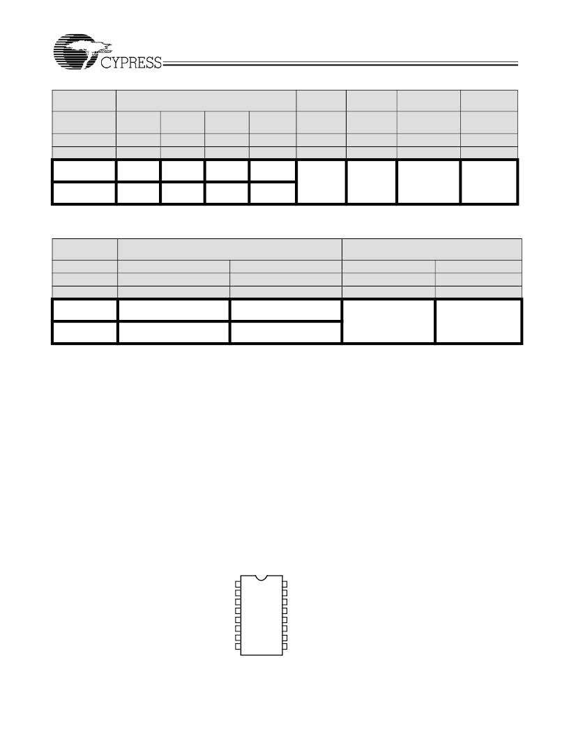
Table 1. Fixed Function Pins
Pin
Function
Pin Name
Output Clock Functions and Frequency
SSCLK1
SSCLK2
Input
Frequency
XIN and
XOUT
1 and 16
MHz
C
XIN
and
C
XOUT
XIN and
XOUT
1 and 16
pF
Spread
Percent
SSCLK[1:6]
Frequency
Modulation
SSCLK[1:6]
SSCLK3
SSCLK4
Pin#
Units
7
8
9
12
MHz
ENTER
DATA
ENTER
DATA
7,8,9,12,14,15 7,8,9,12,14,15
%
MHz
ENTER
DATA
ENTER
DATA
MHz
ENTER
DATA
ENTER
DATA
MHz
ENTER
DATA
ENTER
DATA
kHz
Program Value
CLKSEL = 0
Program Value
CLKSEL = 1
ENTER
DATA
ENTER
DATA
ENTER
DATA
31.5
Table 2. Multi-function Pins
Pin
Function
Pin Name
Pin#
Units
Program Value
CLKSEL = 0
Program Value
CLKSEL = 1
Output Clock /REFOUT /OE/SSON/CLKSEL
SSCLK5/REFOUT/CP2
14
MHz
ENTER DATA
OE/PD#/SSON/CLKSEL
CP0
4
N/A
SSCLK6/REFOUT/CP3
15
MHz
ENTER DATA
CP1
10
N/A
ENTER DATA
ENTER DATA
ENTER DATA
ENTER DATA
1
2
3
4
5
6
7
8
9
10
11
12
13
14
15
16
VSS
VSSL
OE
100MHz
100MHz
33.0MHz
VDD
AVDD
NC
PD#
AVSS
100MHz
SSON
REFOUT(33.0MHz)
VDDL
100MHz
Figure 1.
相關(guān)PDF資料 |
PDF描述 |
|---|---|
| CY25200ZXC | Paired Cable; Number of Conductors:24; Conductor Size AWG:24; No. Strands x Strand Size:7 x 32; Jacket Material:Polyvinylchloride (PVC); Number of Pairs:12; Conductor Material:Copper; Features:Traditional Analog Audio Applications RoHS Compliant: Yes |
| CY25566 | Spread Spectrum Clock Generator |
| CY25566SCT | Spread Spectrum Clock Generator |
| CY25566SC | Spread Spectrum Clock Generator |
| CY25702XZZZ | Programmable High-Frequency Crystal Oscillator (XO) |
相關(guān)代理商/技術(shù)參數(shù) |
參數(shù)描述 |
|---|---|
| CY25200_07 | 制造商:CYPRESS 制造商全稱:Cypress Semiconductor 功能描述:Programmable Spread Spectrum Clock Generator for EMI Reduction |
| CY25200_09 | 制造商:CYPRESS 制造商全稱:Cypress Semiconductor 功能描述:Programmable Spread Spectrum Clock Generator for EMI Reduction |
| CY25200_12 | 制造商:CYPRESS 制造商全稱:Cypress Semiconductor 功能描述:Programmable Spread Spectrum Clock Generator for EMI Reduction |
| CY25200FZXC | 功能描述:鎖相環(huán) - PLL Spectrum Clk Genratr COM RoHS:否 制造商:Silicon Labs 類型:PLL Clock Multiplier 電路數(shù)量:1 最大輸入頻率:710 MHz 最小輸入頻率:0.002 MHz 輸出頻率范圍:0.002 MHz to 808 MHz 電源電壓-最大:3.63 V 電源電壓-最小:1.71 V 最大工作溫度:+ 85 C 最小工作溫度:- 40 C 封裝 / 箱體:QFN-36 封裝:Tray |
| CY25200FZXCT | 功能描述:鎖相環(huán) - PLL Spectrum Clk Genratr COM RoHS:否 制造商:Silicon Labs 類型:PLL Clock Multiplier 電路數(shù)量:1 最大輸入頻率:710 MHz 最小輸入頻率:0.002 MHz 輸出頻率范圍:0.002 MHz to 808 MHz 電源電壓-最大:3.63 V 電源電壓-最小:1.71 V 最大工作溫度:+ 85 C 最小工作溫度:- 40 C 封裝 / 箱體:QFN-36 封裝:Tray |
發(fā)布緊急采購,3分鐘左右您將得到回復(fù)。