- 您現(xiàn)在的位置:買賣IC網(wǎng) > PDF目錄378985 > CXD3008Q (Sony Corporation) CD Digital Signal Processor with Built-in Digital Servo PDF資料下載
參數(shù)資料
| 型號: | CXD3008Q |
| 廠商: | Sony Corporation |
| 元件分類: | 數(shù)字信號處理 |
| 英文描述: | CD Digital Signal Processor with Built-in Digital Servo |
| 中文描述: | CD數(shù)字信號處理器的內(nèi)置數(shù)碼舵機(jī) |
| 文件頁數(shù): | 119/131頁 |
| 文件大小: | 1003K |
| 代理商: | CXD3008Q |
第1頁第2頁第3頁第4頁第5頁第6頁第7頁第8頁第9頁第10頁第11頁第12頁第13頁第14頁第15頁第16頁第17頁第18頁第19頁第20頁第21頁第22頁第23頁第24頁第25頁第26頁第27頁第28頁第29頁第30頁第31頁第32頁第33頁第34頁第35頁第36頁第37頁第38頁第39頁第40頁第41頁第42頁第43頁第44頁第45頁第46頁第47頁第48頁第49頁第50頁第51頁第52頁第53頁第54頁第55頁第56頁第57頁第58頁第59頁第60頁第61頁第62頁第63頁第64頁第65頁第66頁第67頁第68頁第69頁第70頁第71頁第72頁第73頁第74頁第75頁第76頁第77頁第78頁第79頁第80頁第81頁第82頁第83頁第84頁第85頁第86頁第87頁第88頁第89頁第90頁第91頁第92頁第93頁第94頁第95頁第96頁第97頁第98頁第99頁第100頁第101頁第102頁第103頁第104頁第105頁第106頁第107頁第108頁第109頁第110頁第111頁第112頁第113頁第114頁第115頁第116頁第117頁第118頁當(dāng)前第119頁第120頁第121頁第122頁第123頁第124頁第125頁第126頁第127頁第128頁第129頁第130頁第131頁
– 119 –
CXD3008Q
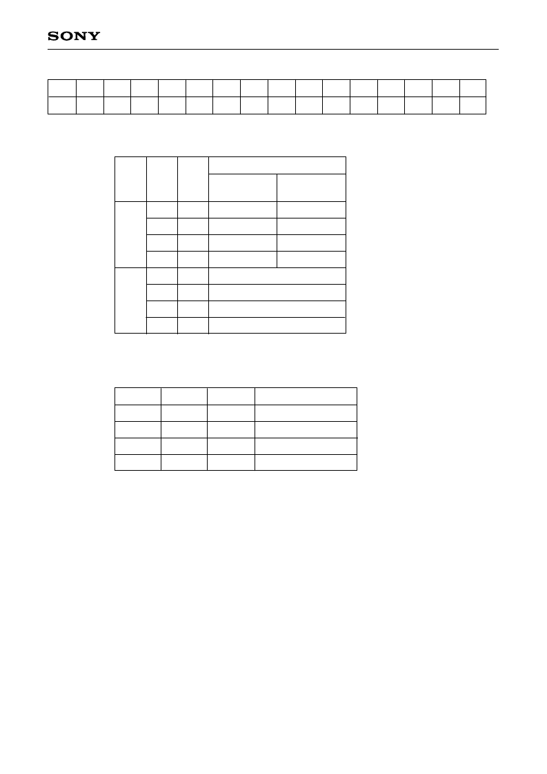
$3F (preset: $3F 00 00)
D15
D14
D13
D12
D11
D10
D9
D8
D7
D6
D5
D4
D3
D2
D1
D0
0
AGG4 XT4D XT2D
0
DRR2 DRR1 DRR0
0
ASFG FTQ LPAS
0
0
AGHF
0
XT4D, XT2D:
MCK (digital servo master clock) frequency division setting
This command forcibly sets the frequency division ratio to 1/4, 1/2 or 1/1 when MCK is
generated. See the description of $3E for XT1D. Also, see the decription of "§5-2. Digital
Servo Block Master Clock (MCK)".
AGG4:
This varies the amplitude of the internally generated sine wave using the AGGF and AGGT
commands during AGC. When AGG4 = 0, the default is used. When AGG4 = 1, the setting is
as shown in the table below.
AGG4
0
1
AGGF
0
1
—
—
0
0
1
1
AGGT
—
—
0
1
0
1
0
1
FE input
conversion
1/36
×
V
DD
×
0.4
1/16
×
V
DD
×
0.4
—
—
TE input
conversion
—
—
1/16
×
V
DD
×
0.4
1/8
×
V
DD
×
0.4
DRR2 to DRR0
: Partially clears the Data RAM values (0 write).
The following values are cleared when 1 (on) respectively; default = 0
DRR2: M08, M09, M0A
DRR1: M00, M01, M02
DRR0: M00, M01, M02 only when LOCK = low
Note)
Set DRR1 and DRR0 on for 50μs or more.
ASFG:
When vibration detection is performed during anti-shock circuit operation, the FCS servo filter
is forcibly set to gain normal status.
On when 1; default when 0
LPAS:
Built-in analog buffer low-current consumption mode
This mode reduces the total analog buffer current consumption for the VC, TE, SE and FE
input analog buffers by using a single operational amplifier.
On when 1; default when 0
Note)
When using this mode, first check whether each error signal is properly A/D converted
using the data readout and the like.
AGHF:
This halves the frequency of the internally generated sine wave during AGC.
FTQ:
The slope of the output during focus search is 1/4 of the conventional output slope.
On when 1; default when 0 .
ASOT:
The anti-shock signal, which is internally detected, is output from the ATSK pin.
Output when set to 1; default = 0
Vibration detection when a high signal is output for the anti-shock signal output.
See $37 for AGGF and AGGT.
The presets are AGG4 = 0,
AGGF = 1 and AGGT = 1.
: preset, —: don't care
: preset, —: don't care
XT1D
0
1
0
0
XT2D
0
—
1
0
XT4D
0
—
—
1
According to XTSL
1/1
1/2
1/4
Frequency division ratio
Sine wave amplitude
1/64
×
V
DD
×
0.4
1/32
×
V
DD
×
0.4
1/16
×
V
DD
×
0.4
1/8
×
V
DD
×
0.4
相關(guān)PDF資料 |
PDF描述 |
|---|---|
| CXD3009Q | CD Digital Signal Processor(CD數(shù)字信號處理器) |
| CXD3011R-1 | Hook-Up Wire; Conductor Size AWG:26; No. Strands x Strand Size:7 x 34; Jacket Color:White/Yellow; Cable/Wire MIL SPEC:MIL-W-16878/1 Type B; Conductor Material:Copper; Jacket Material:Polyvinylchloride (PVC) RoHS Compliant: Yes |
| CXD3017Q | CD Digital Signal Processor with Built-in Digital Servo and DAC(CD數(shù)字信號處理器(內(nèi)置數(shù)字伺服系統(tǒng)和 D/A轉(zhuǎn)換器)) |
| CXD3027R | CD Digital Signal Processor with Built-in Digital Servo +Shock-Proof Memory Controller + Digital High & Bass Boost(CD數(shù)字信號處理器(內(nèi)置數(shù)字伺服系統(tǒng)、防震存儲器控制器、數(shù)字式高&低音提升電路)) |
| cxd3027 | CD Audio Digital Signal-Processing LSI Device with On-Chip Digital Servo System Allows Listening without Sound Skipping |
相關(guān)代理商/技術(shù)參數(shù) |
參數(shù)描述 |
|---|---|
| CXD3009Q | 制造商:SONY 制造商全稱:Sony Corporation 功能描述:CD Digital Signal Processor |
| CXD3011R-1 | 制造商:SONY 制造商全稱:Sony Corporation 功能描述:CD Digital Signal Processor with Built-in Digital Servo and DAC |
| CXD3017Q | 制造商:SONY 制造商全稱:Sony Corporation 功能描述:CD Digital Signal Processor with Built-in Digital Servo and DAC |
| CXD3018Q/R | 制造商:未知廠家 制造商全稱:未知廠家 功能描述:CD Digital Signal Processor with Built-in DigitalServo and DAC |
| CXD3021 | 制造商:SONY 制造商全稱:Sony Corporation 功能描述:CD Digital Signal Processor with Built-in Digital Servo and DAC |
發(fā)布緊急采購,3分鐘左右您將得到回復(fù)。