- 您現(xiàn)在的位置:買賣IC網(wǎng) > PDF目錄3768 > CS82C55A96 (Intersil)IC I/O EXPANDER 24B 44PLCC PDF資料下載
參數(shù)資料
| 型號(hào): | CS82C55A96 |
| 廠商: | Intersil |
| 文件頁(yè)數(shù): | 24/29頁(yè) |
| 文件大小: | 0K |
| 描述: | IC I/O EXPANDER 24B 44PLCC |
| 標(biāo)準(zhǔn)包裝: | 500 |
| 接口: | 可編程 |
| 輸入/輸出數(shù): | 24 |
| 中斷輸出: | 無(wú) |
| 電源電壓: | 4.5 V ~ 5.5 V |
| 工作溫度: | 0°C ~ 70°C |
| 安裝類型: | 表面貼裝 |
| 封裝/外殼: | 44-LCC(J 形引線) |
| 供應(yīng)商設(shè)備封裝: | 44-PLCC |
| 包裝: | 管件 |
第1頁(yè)第2頁(yè)第3頁(yè)第4頁(yè)第5頁(yè)第6頁(yè)第7頁(yè)第8頁(yè)第9頁(yè)第10頁(yè)第11頁(yè)第12頁(yè)第13頁(yè)第14頁(yè)第15頁(yè)第16頁(yè)第17頁(yè)第18頁(yè)第19頁(yè)第20頁(yè)第21頁(yè)第22頁(yè)第23頁(yè)當(dāng)前第24頁(yè)第25頁(yè)第26頁(yè)第27頁(yè)第28頁(yè)第29頁(yè)

4
FN2969.10
November 16, 2006
Functional Description
Data Bus Buffer
This three-state bidirectional 8-bit buffer is used to interface
the 82C55A to the system data bus. Data is transmitted or
received by the buffer upon execution of input or output
instructions by the CPU. Control words and status
information are also transferred through the data bus buffer.
Read/Write and Control Logic
The function of this block is to manage all of the internal and
external transfers of both Data and Control or Status words.
It accepts inputs from the CPU Address and Control busses
and in turn, issues commands to both of the Control Groups.
(CS) Chip Select. A “l(fā)ow” on this input pin enables the
communication between the 82C55A and the CPU.
(RD) Read. A “l(fā)ow” on this input pin enables 82C55A to send
the data or status information to the CPU on the data bus. In
essence, it allows the CPU to “read from” the 82C55A.
(WR) Write. A “l(fā)ow” on this input pin enables the CPU to
write data or control words into the 82C55A.
(A0 and A1) Port Select 0 and Port Select 1. These input
signals, in conjunction with the RD and WR inputs, control
the selection of one of the three ports or the control word
register. They are normally connected to the least significant
bits of the address bus (A0 and A1).
(RESET) Reset. A “high” on this input initializes the control
register to 9Bh and all ports (A, B, C) are set to the input
mode. “Bus hold” devices internal to the 82C55A will hold
the I/O port inputs to a logic “1” state with a maximum hold
current of 400
μA.
Group A and Group B Controls
The functional configuration of each port is programmed by
the systems software. In essence, the CPU “outputs” a
control word to the 82C55A. The control word contains
information such as “mode”, “bit set”, “bit reset”, etc., that
initializes the functional configuration of the 82C55A.
Each of the Control blocks (Group A and Group B) accepts
“commands” from the Read/Write Control logic, receives
“control words” from the internal data bus and issues the
proper commands to its associated ports.
Control Group A - Port A and Port C upper (C7 - C4)
Control Group B - Port B and Port C lower (C3 - C0)
The control word register can be both written and read as
shown in the “Basic Operation” table. Figure 4 shows the
control word format for both Read and Write operations.
When the control word is read, bit D7 will always be a logic
“1”, as this implies control word mode information.
Ports A, B, and C
The 82C55A contains three 8-bit ports (A, B, and C). All can
be configured to a wide variety of functional characteristics
by the system software but each has its own special features
or “personality” to further enhance the power and flexibility of
the 82C55A.
Port A One 8-bit data output latch/buffer and one 8-bit data
input latch. Both “pull-up” and “pull-down” bus-hold devices
are present on Port A. See Figure 2A.
Port B One 8-bit data input/output latch/buffer and one 8-bit
data input buffer. See Figure 2B.
Port C One 8-bit data output latch/buffer and one 8-bit data
input buffer (no latch for input). This port can be divided into
82C55A BASIC OPERATION
A1
A0
RD
WR
CS
INPUT OPERATION
(READ)
00010
Port A
→ Data Bus
01010
Port B
→ Data Bus
10010
Port C
→ Data Bus
11010
Control Word
→ Data Bus
OUTPUT OPERATION
(WRITE)
00100
Data Bus
→ Port A
01100
Data Bus
→ Port B
10100
Data Bus
→ Port C
11100
Data Bus
→ Control
DISABLE FUNCTION
XXXX
1
Data Bus
→ Three-State
X
110
Data Bus
→ Three-State
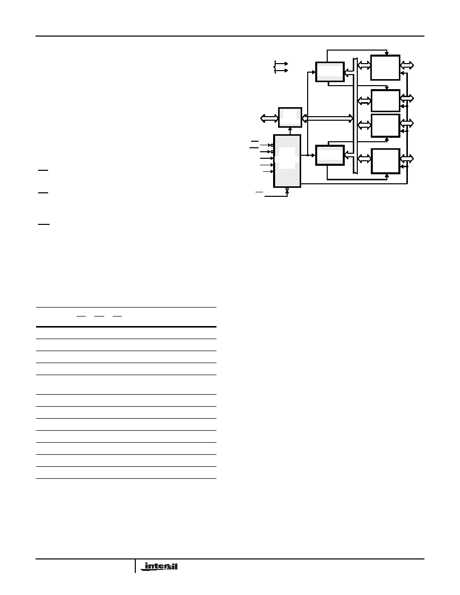
FIGURE 1. 82C55A BLOCK DIAGRAM. DATA BUS BUFFER,
READ/WRITE, GROUP A & B CONTROL LOGIC
FUNCTIONS
GROUP A
PORT A
(8)
GROUP A
PORT C
UPPER
(4)
GROUP B
PORT C
LOWER
(4)
GROUP B
PORT B
(8)
GROUP B
CONTROL
GROUP A
CONTROL
DATA
READ
WRITE
CONTROL
LOGIC
RD
WR
A1
A0
RESET
CS
D7-D0
POWER
SUPPLIES
+5V
GND
BIDIRECTIONAL
DATA BUS
I/O
PA7-
I/O
PC7-
I/O
PC3-
I/O
PB7-
BUFFER
BUS
PB0
PC0
PC4
PA0
8-BIT
INTERNAL
DATA BUS
82C55A
相關(guān)PDF資料 |
PDF描述 |
|---|---|
| IS82C55A-5Z96 | IC I/O EXPANDER 24B 44PLCC |
| ATMEGA8535-16AUR | MCU AVR 8K FLASH 16MHZ 44TQFP |
| IS82C55A-5Z | IC I/O EXPANDER 24B 44PLCC |
| CS82C55A-596 | IC I/O EXPANDER 24B 44PLCC |
| CS82C55A-5 | IC I/O EXPANDER 24B 44PLCC |
相關(guān)代理商/技術(shù)參數(shù) |
參數(shù)描述 |
|---|---|
| CS82C55A96S2580 | 制造商:Rochester Electronics LLC 功能描述:- Bulk |
| CS82C55A96S5001 | 制造商:Intersil Corporation 功能描述: |
| CS82C55AR2490 | 制造商:Rochester Electronics LLC 功能描述:- Bulk |
| CS82C55AS2507 | 制造商:Rochester Electronics LLC 功能描述:- Bulk |
| CS82C55AZ | 功能描述:外圍驅(qū)動(dòng)器與原件 - PCI PERI PRG-I/O 5V 8MHZ 44PLCC COM RoHS:否 制造商:PLX Technology 工作電源電壓: 最大工作溫度: 安裝風(fēng)格:SMD/SMT 封裝 / 箱體:FCBGA-1156 封裝:Tray |
發(fā)布緊急采購(gòu),3分鐘左右您將得到回復(fù)。