- 您現(xiàn)在的位置:買賣IC網(wǎng) > PDF目錄378449 > CMT10N10 (Electronic Theatre Controls, Inc.) POWER FIELD EFFECT TRANSISTOR PDF資料下載
參數(shù)資料
| 型號(hào): | CMT10N10 |
| 廠商: | Electronic Theatre Controls, Inc. |
| 英文描述: | POWER FIELD EFFECT TRANSISTOR |
| 中文描述: | 功率場效應(yīng)晶體管 |
| 文件頁數(shù): | 1/5頁 |
| 文件大?。?/td> | 168K |
| 代理商: | CMT10N10 |
CMT10N10
P
OWER
F
IELD
E
FFECT
T
RANSISTOR
2001/12/24
Preliminary
Rev. 1
Champion Microelectronic Corporation
Page 1
GENERAL DESCRIPTION
This advanced MOSFET is designed to withstand high
energy in avalanche and commutation modes. The new
energy efficient design also offers a drain-to-source diode
with a fast recovery time. Designed for high voltage, high
speed switching applications in power supplies, converters
and PWM motor controls, these devices are particularly well
suited for bridge circuits where diode speed and
commutating safe operating areas are critical and offer
additional and safety margin against unexpected voltage
transients.
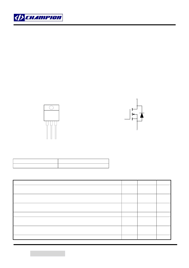
PIN CONFIGURATION
TO-220
Front View
FEATURES
!
Avalanche Energy Specified
!
Source-to-Drain Diode Recovery Time Comparable to a
Discrete Fast Recovery Diode
!
Diode is Characterized for Use in Bridge Circuits
!
I
DSS
and V
DS
(on) Specified at Elevated Temperature
SYMBOL
1
2
3
G
D
S
ORDERING INFORMATION
Part Number
CMT10N10N220
ABSOLUTE MAXIMUM RATINGS
D
S
G
N-Channel MOSFET
Package
TO-220
Rating
Symbol
I
D
I
DM
V
GS
V
GSM
P
D
Value
10
35
±20
±40
40
0.32
-55 to 150
69
3.13
100
260
Unit
A
V
V
W
W/
℃
℃
mJ
Drain to Current
-
Continuous
-
Pulsed
Gate-to-Source Voltage
-
Continue
-
Non-repetitive
Total Power Dissipation
Derate above 25
℃
Operating and Storage Temperature Range
Single Pulse Drain-to-Source Avalanche Energy
-
T
J
= 25
℃
(V
DD
= 100V, V
GS
= 10V, I
L
= 10A, L = 1.38mH, R
G
= 25
)
Thermal Resistance
-
Junction to Case
-
Junction to Ambient
Maximum Lead Temperature for Soldering Purposes, 1/8” from case for 10 seconds
T
J
, T
STG
E
AS
θ
JC
θ
JA
T
L
℃
/W
℃
相關(guān)PDF資料 |
PDF描述 |
|---|---|
| CMT10N10N220 | POWER FIELD EFFECT TRANSISTOR |
| CMT18N20 | POWER FIELD EFFECT TRANSISTOR |
| CMT18N20N220 | POWER FIELD EFFECT TRANSISTOR |
| cmy 800 | GaAs MMIC(砷化鎵微波放大器) |
| CMY213 | GaAs MMIC |
相關(guān)代理商/技術(shù)參數(shù) |
參數(shù)描述 |
|---|---|
| CMT10N10N220 | 制造商:未知廠家 制造商全稱:未知廠家 功能描述:POWER FIELD EFFECT TRANSISTOR |
| CMT10N40 | 制造商:未知廠家 制造商全稱:未知廠家 功能描述:POWER MOSFET |
| CMT10N40N220 | 制造商:未知廠家 制造商全稱:未知廠家 功能描述:POWER MOSFET |
| CMT1-1 | 制造商:COOPER BUSSMANN 功能描述:Common Mode Chokes Dual 66mH 10kHz 740mA Thru-Hole Bulk |
| CMT1-1.0-6 | 制造商:Coilcraft Inc 功能描述:NOT RoHS. Common mode choke, toroid (add 'L' for compliant version) |
發(fā)布緊急采購,3分鐘左右您將得到回復(fù)。