- 您現(xiàn)在的位置:買(mǎi)賣(mài)IC網(wǎng) > PDF目錄227831 > CAT93C76VI-REVA 512 X 16 MICROWIRE BUS SERIAL EEPROM, PDSO8 PDF資料下載
參數(shù)資料
| 型號(hào): | CAT93C76VI-REVA |
| 元件分類(lèi): | PROM |
| 英文描述: | 512 X 16 MICROWIRE BUS SERIAL EEPROM, PDSO8 |
| 封裝: | SOIC-8 |
| 文件頁(yè)數(shù): | 3/10頁(yè) |
| 文件大小: | 412K |
| 代理商: | CAT93C76VI-REVA |
2
CAT93C76
Doc. No. 1090, Rev. A
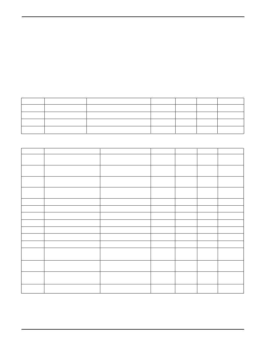
D.C. OPERATING CHARACTERISTICS
VCC = +1.8V to +5.5V, unless otherwise specified.
Symbol
Parameter
Test Conditions
Min
Typ
Max
Units
ICC1
Power Supply Current
fSK = 1MHz
1
3
mA
(Write)
VCC = 5.0V
ICC2
Power Supply Current
fSK = 1MHz
300
500
A
(Read)
VCC = 5.0V
ISB1
Power Supply Current
CS = 0V
2
10
A
(Standby) (x8 Mode)
ORG=GND
ISB2
Power Supply Current
CS=0V
0(5)
10
A
(Standby) (x16Mode)
ORG=Float or VCC
ILI
Input Leakage Current
VIN = 0V to VCC
0(5)
10
A
ILO
Output Leakage Current
VOUT = 0V to VCC, CS = 0V
0(5)
10
A
ILORG
ORG Pin Leakage Current
ORG = GND or ORG = VCC
110
A
VIL1
Input Low Voltage
4.5V
≤ VCC ≤ 5.5V
-0.1
0.8
V
VIH1
Input High Voltage
4.5V
≤ VCC ≤ 5.5V
2
VCC + 1
V
VIL2
Input Low Voltage
1.8V
≤ VCC < 4.5V
0
VCC x 0.2
V
VIH2
Input High Voltage
1.8V
≤ VCC < 4.5V
VCC x 0.7
VCC+1
V
VOL1
Output Low Voltage
4.5V
≤ VCC ≤ 5.5V
0.4
V
IOL = 2.1mA
VOH1
Output High Voltage
4.5V
≤ VCC ≤ 5.5V
2.4
V
IOH = -400
A
VOL2
Output Low Voltage
1.8V
≤ VCC < 4.5V
0.1
V
IOL = 100
A
VOH2
Output High Voltage
1.8V
≤ VCC < 4.5V
VCC - 0.2
V
IOH = -100
A
ABSOLUTE MAXIMUM RATINGS*
Temperature Under Bias .................. -55
°C to +125°C
Storage Temperature ........................ -65
°C to +150°C
Voltage on any Pin with
Respect to Ground(1) ............. -2.0V to +VCC +2.0V
VCC with Respect to Ground ................ -2.0V to +7.0V
Lead Soldering Temperature (10 secs) ............ 300
°C
Output Short Circuit Current(2) ........................ 100 mA
*COMMENT
Stresses exceeding those listed under “Absolute Maxi-
mum Ratings” may cause permanent damage to the
device. These are stress ratings only, and functional
operation of the device at these or any other conditions
outside of those listed in the operational sections of this
specification is not implied. Exposure to any absolute
maximum rating for extended periods may affect device
performance and reliability.
RELIABILITY CHARACTERISTICS
Symbol
Parameter
Reference Test Method
Min
Typ
Max
Units
NEND(3)
Endurance
MIL-STD-883, Test Method 1033
1,000,000
Cycles/Byte
TDR(3)
Data Retention
MIL-STD-883, Test Method 1008
100
Years
VZAP(3)
ESD Susceptibility
MIL-STD-883, Test Method 3015
2000
Volts
ILTH(3)(4)
Latch-Up
JEDEC Standard 17
100
mA
Note:
(1) The minimum DC input voltage is –0.5V. During transitions, inputs may undershoot to –2.0V for periods of less than 20 ns. Maximum DC
voltage on output pins is VCC +0.5V, which may overshoot to VCC +2.0V for periods of less than 20 ns.
(2) Output shorted for no more than one second.
(3) These parameters are tested initially and after a design or process change that affects the parameter.
(4) Latch-up protection is provided for stresses up to 100 mA on I/O pins from –1V to VCC +1V.
(5) 0
A is defined as less than 900 nA.
相關(guān)PDF資料 |
PDF描述 |
|---|---|
| CY7C1031-10NC | 64K X 18 CACHE SRAM, 10 ns, PQFP52 |
| CAT93C86W-1.8 | 1K X 16 MICROWIRE BUS SERIAL EEPROM, PDSO8 |
| CAT93C86KI-TE13 | 1K X 16 MICROWIRE BUS SERIAL EEPROM, PDSO8 |
| CAT93C86JA-TE13 | 1K X 16 MICROWIRE BUS SERIAL EEPROM, PDSO8 |
| CAT24WC03YE-1.8TE13REV-C | 256 X 8 I2C/2-WIRE SERIAL EEPROM, PDSO8 |
相關(guān)代理商/技術(shù)參數(shù) |
參數(shù)描述 |
|---|---|
| CAT93C76WGI | 制造商:Rochester Electronics LLC 功能描述: 制造商:Catalyst Semiconductor 功能描述: |
| CAT93C76YGI | 制造商:Rochester Electronics LLC 功能描述: 制造商:Catalyst Semiconductor 功能描述: |
| CAT93C76YGI-T3 | 制造商:Rochester Electronics LLC 功能描述: 制造商:Catalyst Semiconductor 功能描述: |
| CAT93C76YI-G | 功能描述:電可擦除可編程只讀存儲(chǔ)器 (1024x8)/(512x16) 8K RoHS:否 制造商:Atmel 存儲(chǔ)容量:2 Kbit 組織:256 B x 8 數(shù)據(jù)保留:100 yr 最大時(shí)鐘頻率:1000 KHz 最大工作電流:6 uA 工作電源電壓:1.7 V to 5.5 V 最大工作溫度:+ 85 C 安裝風(fēng)格:SMD/SMT 封裝 / 箱體:SOIC-8 |
| CAT93C76YI-GT3 | 功能描述:電可擦除可編程只讀存儲(chǔ)器 8K-Bit Microwire Serial 電可擦除可編程只讀存儲(chǔ)器 RoHS:否 制造商:Atmel 存儲(chǔ)容量:2 Kbit 組織:256 B x 8 數(shù)據(jù)保留:100 yr 最大時(shí)鐘頻率:1000 KHz 最大工作電流:6 uA 工作電源電壓:1.7 V to 5.5 V 最大工作溫度:+ 85 C 安裝風(fēng)格:SMD/SMT 封裝 / 箱體:SOIC-8 |
發(fā)布緊急采購(gòu),3分鐘左右您將得到回復(fù)。