- 您現(xiàn)在的位置:買(mǎi)賣(mài)IC網(wǎng) > PDF目錄295214 > CAT130041SWI-GT3 1-CHANNEL POWER SUPPLY SUPPORT CKT, PDSO8 PDF資料下載
參數(shù)資料
| 型號(hào): | CAT130041SWI-GT3 |
| 元件分類: | 電源管理 |
| 英文描述: | 1-CHANNEL POWER SUPPLY SUPPORT CKT, PDSO8 |
| 封裝: | 0.150 INCH, ROHS COMPLIANT, MS-012, SOIC-8 |
| 文件頁(yè)數(shù): | 12/14頁(yè) |
| 文件大小: | 310K |
| 代理商: | CAT130041SWI-GT3 |
第1頁(yè)第2頁(yè)第3頁(yè)第4頁(yè)第5頁(yè)第6頁(yè)第7頁(yè)第8頁(yè)第9頁(yè)第10頁(yè)第11頁(yè)當(dāng)前第12頁(yè)第13頁(yè)第14頁(yè)

CAT130xx
2007 Catalyst Semiconductor, Inc.
7
Doc. No. 1121 Rev. A
Characteristics subject to change without notice
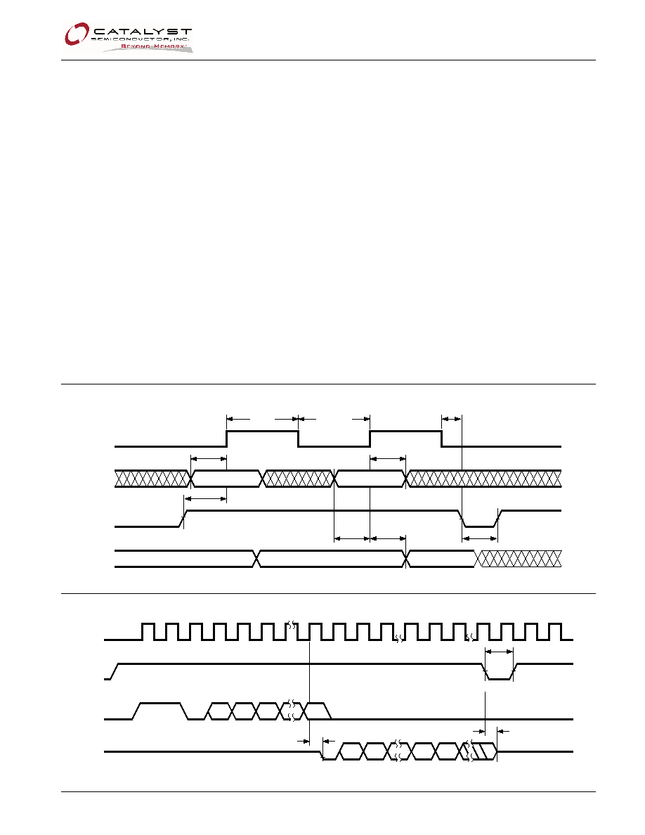
Instructions, addresses, and write data are clocked
into the DI pin on the rising edge of the clock (SK).
The DO pin is normally in a high impedance state
except when reading data from the device, or when
checking the ready/busy status during a write
operation. The serial communication protocol follows
the timing shown in Figure 3.
The ready/busy status can be determined after the
start of internal write cycle by selecting the device (CS
high) and polling the DO pin; DO low indicates that the
write operation is not completed, while DO high
indicates that the device is ready for the next
instruction. If necessary, the DO pin may be placed
back into a high impedance state during chip select by
shifting a dummy “1” into the DI pin. The DO pin will
enter the high impedance state on the rising edge of
the clock (SK). Placing the DO pin into the high
impedance state is recommended in applications
where the DI pin and the DO pin are to be tied
together to form a common DI/O pin. The Ready/Busy
flag can be disabled only in Ready state; no change is
allowed in Busy state.
Read
Upon receiving a READ command and an address
(clocked into the DI pin), the DO pin of the CAT130xx
will come out of the high impedance state and, after
sending an initial dummy zero bit, will begin shifting
out the data addressed (MSB first). The output data
bits will toggle on the rising edge of the SK clock and
are stable after the specified time delay (tPD0 or tPD1).
The READ instruction timing is illustrated in Figure 4.
For the CAT13004/08/16, after the initial data word
has been shifted out and CS remains asserted with
the SK clock continuing to toggle, the device will auto-
matically increment to the next address and shift out
the next data word in a sequential READ mode. As
long as CS is continuously asserted and SK continues
to toggle, the device will keep incrementing to the next
address automatically until it reaches to the end of the
address space, then loops back to address 0. In the
sequential READ mode, only the initial data word is
preceeded by a dummy zero bit. All subsequent data
words will follow without a dummy zero bit.
Figure 3. Sychronous Data Timing
Figure 4. Read Instruction Timing
SK
DI
CS
DO
tDIS
tPD0,tPD1
tCSMIN
tCSS
tDIS
tDIH
tSKHI
tCSH
VALID
DATA VALID
tSKLOW
SK
CS
DI
DO
tCSMIN
tHZ
HIGH-Z
11
0
AN AN-1
A0
0
DN DN-1
D1
D0
tPD0
相關(guān)PDF資料 |
PDF描述 |
|---|---|
| CAT150089RWI-GT3 | 8K X 1 SPI BUS SERIAL EEPROM, PDSO8 |
| CAT150169RWI-GT3 | 16K X 1 SPI BUS SERIAL EEPROM, PDSO8 |
| CAT1641UI-45TE13 | 1-CHANNEL POWER SUPPLY SUPPORT CKT, PDSO8 |
| CAT1641JI-25 | 1-CHANNEL POWER SUPPLY SUPPORT CKT, PDSO8 |
| CAT1641RD2I-42TE13 | 1-CHANNEL POWER SUPPLY SUPPORT CKT, DSO8 |
相關(guān)代理商/技術(shù)參數(shù) |
參數(shù)描述 |
|---|---|
| CAT1320LI25 | 制造商:ON Semiconductor 功能描述:CPU SUPERVISOR WITH 32K EEPROM - Rail/Tube |
| CAT1320LI-25-G | 功能描述:監(jiān)控電路 CPU w/32K RoHS:否 制造商:STMicroelectronics 監(jiān)測(cè)電壓數(shù): 監(jiān)測(cè)電壓: 欠電壓閾值: 過(guò)電壓閾值: 輸出類型:Active Low, Open Drain 人工復(fù)位:Resettable 監(jiān)視器:No Watchdog 電池備用開(kāi)關(guān):No Backup 上電復(fù)位延遲(典型值):10 s 電源電壓-最大:5.5 V 最大工作溫度:+ 85 C 安裝風(fēng)格:SMD/SMT 封裝 / 箱體:UDFN-6 封裝:Reel |
| CAT1320LI28 | 制造商:ON Semiconductor 功能描述:CPU SUPERVISOR WITH 32K EEPROM - Rail/Tube |
| CAT1320LI-28-G | 功能描述:監(jiān)控電路 CPU w/32K RoHS:否 制造商:STMicroelectronics 監(jiān)測(cè)電壓數(shù): 監(jiān)測(cè)電壓: 欠電壓閾值: 過(guò)電壓閾值: 輸出類型:Active Low, Open Drain 人工復(fù)位:Resettable 監(jiān)視器:No Watchdog 電池備用開(kāi)關(guān):No Backup 上電復(fù)位延遲(典型值):10 s 電源電壓-最大:5.5 V 最大工作溫度:+ 85 C 安裝風(fēng)格:SMD/SMT 封裝 / 箱體:UDFN-6 封裝:Reel |
| CAT1320LI30 | 制造商:ON Semiconductor 功能描述:CPU SUPERVISOR WITH 32K EEPROM - Rail/Tube |
發(fā)布緊急采購(gòu),3分鐘左右您將得到回復(fù)。