- 您現(xiàn)在的位置:買(mǎi)賣(mài)IC網(wǎng) > PDF目錄255752 > BX80524P500128 (INTEL CORP) 32-BIT, 500 MHz, MICROPROCESSOR, PPGA370 PDF資料下載
參數(shù)資料
| 型號(hào): | BX80524P500128 |
| 廠商: | INTEL CORP |
| 元件分類(lèi): | 微控制器/微處理器 |
| 英文描述: | 32-BIT, 500 MHz, MICROPROCESSOR, PPGA370 |
| 封裝: | 1.950 X 1.950 INCH, HEAT SINK, STAGGERED, PLASTIC, PGA-370 |
| 文件頁(yè)數(shù): | 28/130頁(yè) |
| 文件大小: | 2654K |
| 代理商: | BX80524P500128 |
第1頁(yè)第2頁(yè)第3頁(yè)第4頁(yè)第5頁(yè)第6頁(yè)第7頁(yè)第8頁(yè)第9頁(yè)第10頁(yè)第11頁(yè)第12頁(yè)第13頁(yè)第14頁(yè)第15頁(yè)第16頁(yè)第17頁(yè)第18頁(yè)第19頁(yè)第20頁(yè)第21頁(yè)第22頁(yè)第23頁(yè)第24頁(yè)第25頁(yè)第26頁(yè)第27頁(yè)當(dāng)前第28頁(yè)第29頁(yè)第30頁(yè)第31頁(yè)第32頁(yè)第33頁(yè)第34頁(yè)第35頁(yè)第36頁(yè)第37頁(yè)第38頁(yè)第39頁(yè)第40頁(yè)第41頁(yè)第42頁(yè)第43頁(yè)第44頁(yè)第45頁(yè)第46頁(yè)第47頁(yè)第48頁(yè)第49頁(yè)第50頁(yè)第51頁(yè)第52頁(yè)第53頁(yè)第54頁(yè)第55頁(yè)第56頁(yè)第57頁(yè)第58頁(yè)第59頁(yè)第60頁(yè)第61頁(yè)第62頁(yè)第63頁(yè)第64頁(yè)第65頁(yè)第66頁(yè)第67頁(yè)第68頁(yè)第69頁(yè)第70頁(yè)第71頁(yè)第72頁(yè)第73頁(yè)第74頁(yè)第75頁(yè)第76頁(yè)第77頁(yè)第78頁(yè)第79頁(yè)第80頁(yè)第81頁(yè)第82頁(yè)第83頁(yè)第84頁(yè)第85頁(yè)第86頁(yè)第87頁(yè)第88頁(yè)第89頁(yè)第90頁(yè)第91頁(yè)第92頁(yè)第93頁(yè)第94頁(yè)第95頁(yè)第96頁(yè)第97頁(yè)第98頁(yè)第99頁(yè)第100頁(yè)第101頁(yè)第102頁(yè)第103頁(yè)第104頁(yè)第105頁(yè)第106頁(yè)第107頁(yè)第108頁(yè)第109頁(yè)第110頁(yè)第111頁(yè)第112頁(yè)第113頁(yè)第114頁(yè)第115頁(yè)第116頁(yè)第117頁(yè)第118頁(yè)第119頁(yè)第120頁(yè)第121頁(yè)第122頁(yè)第123頁(yè)第124頁(yè)第125頁(yè)第126頁(yè)第127頁(yè)第128頁(yè)第129頁(yè)第130頁(yè)
Datasheet
123
Intel Celeron Processor up to 1.10 GHz
LINT[1:0]
I
The LINT[1:0] (Local APIC Interrupt) signals must connect the appropriate pins of all
APIC Bus agents, including all processors and the core logic or I/O APIC
component. When the APIC is disabled, the LINT0 signal becomes INTR, a
maskable interrupt request signal, and LINT1 becomes NMI, a nonmaskable
interrupt. INTR and NMI are backward compatible with the signals of those names
on the Pentium processor. Both signals are asynchronous.
Both of these signals must be software configured via BIOS programming of the
APIC register space to be used either as NMI/INTR or LINT[1:0]. Because the APIC
is enabled by default after Reset, operation of these pins as LINT[1:0] is the default
configuration.
LOCK#
I/O
The LOCK# signal indicates to the system that a transaction must occur atomically.
This signal must connect the appropriate pins of all system bus agents. For a locked
sequence of transactions, LOCK# is asserted from the beginning of the first
transaction end of the last transaction.
When the priority agent asserts BPRI# to arbitrate for ownership of the system bus,
it will wait until it observes LOCK# deasserted. This enables symmetric agents to
retain ownership of the system bus throughout the bus locked operation and ensure
the atomicity of lock.
PICCLK
I
The PICCLK (APIC Clock) signal is an input clock to the processor and core logic or
I/O APIC which is required for operation of all processors, core logic, and I/O APIC
components on the APIC bus.
PICD[1:0]
I/O
The PICD[1:0] (APIC Data) signals are used for bidirectional serial message passing
on the APIC bus, and must connect the appropriate pins of the Intel Celeron
processor for proper initialization.
PLL1, PLL2
(PGA packages
only)
I
All Intel Celeron processors have internal analog PLL clock generators that require
quiet power supplies. PLL1 and PLL2 are inputs to the internal PLL and should be
connected to VCCCORE through a low-pass filter that minimizes jitter. See the
platform design guide for implementation details.
PRDY#
O
The PRDY (Probe Ready) signal is a processor output used by debug tools to
determine processor debug readiness.
PREQ#
I
The PREQ# (Probe Request) signal is used by debug tools to request debug
operation of the processors.
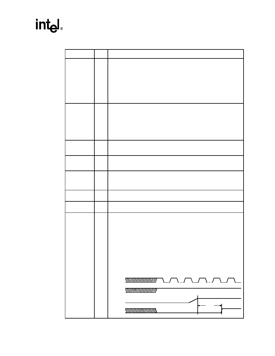
PWRGOOD
I
The PWRGOOD (Power Good) signal is a 2.5 V tolerant processor input. The
processor requires this signal to be a clean indication that the clocks and power
supplies (VCCCORE, etc.) are stable and within their specifications. Clean implies
that the signal will remain low (capable of sinking leakage current), without glitches,
from the time that the power supplies are turned on until they come within
specification. The signal must then transition monotonically to a high (2.5 V) state.
Figure 43 illustrates the relationship of PWRGOOD to other system signals.
PWRGOOD can be driven inactive at any time, but clocks and power must again be
stable before a subsequent rising edge of PWRGOOD. It must also meet the
1ms RESET# pulse.
The PWRGOOD signal must be supplied to the processor; it is used to protect
internal circuits against voltage sequencing issues. It should be driven high
throughout boundary scan operation.
PWRGOOD Relationship at Power-On
Table 59. Alphabetical Signal Reference (Sheet 4 of 7)
Signal
Type
Description
BCLK
PWRGOOD
RESET#
1 ms
VCC
CORE
,
V
REF
相關(guān)PDF資料 |
PDF描述 |
|---|---|
| BU-61582D0-191S | 2 CHANNEL(S), 1M bps, MIL-STD-1553 CONTROLLER, CQIP70 |
| BU-61582D1-121W | 2 CHANNEL(S), 1M bps, MIL-STD-1553 CONTROLLER, CQIP70 |
| BU-61582D1-140K | 2 CHANNEL(S), 1M bps, MIL-STD-1553 CONTROLLER, CQIP70 |
| BU-61582D1-170Q | 2 CHANNEL(S), 1M bps, MIL-STD-1553 CONTROLLER, CQIP70 |
| BU-61582D1-190Q | 2 CHANNEL(S), 1M bps, MIL-STD-1553 CONTROLLER, CQIP70 |
相關(guān)代理商/技術(shù)參數(shù) |
參數(shù)描述 |
|---|---|
| BX80524R30012A | 制造商:未知廠家 制造商全稱(chēng):未知廠家 功能描述:32-Bit Microprocessor |
| BX80524R33312A | 制造商:未知廠家 制造商全稱(chēng):未知廠家 功能描述:32-Bit Microprocessor |
| BX80525U500256E | 制造商:未知廠家 制造商全稱(chēng):未知廠家 功能描述:Microprocessor |
| BX80525U533256EB | 制造商:未知廠家 制造商全稱(chēng):未知廠家 功能描述:Microprocessor |
| BX80525U550256E | 制造商:未知廠家 制造商全稱(chēng):未知廠家 功能描述:Microprocessor |
發(fā)布緊急采購(gòu),3分鐘左右您將得到回復(fù)。