- 您現(xiàn)在的位置:買賣IC網(wǎng) > PDF目錄42906 > AUIRF7648M2TR1 14 A, 60 V, 0.007 ohm, N-CHANNEL, Si, POWER, MOSFET PDF資料下載
參數(shù)資料
| 型號(hào): | AUIRF7648M2TR1 |
| 元件分類: | JFETs |
| 英文描述: | 14 A, 60 V, 0.007 ohm, N-CHANNEL, Si, POWER, MOSFET |
| 封裝: | HALOGEN FREE AND ROHS COMPLIANT PACKAGE-5 |
| 文件頁(yè)數(shù): | 1/11頁(yè) |
| 文件大小: | 290K |
| 代理商: | AUIRF7648M2TR1 |
Description
The AUIRF7648M2 combines the latest Automotive HEXFET Power MOSFET Silicon technology with the advanced DirectFET packaging to
achieve low gate charge as well as the lowest on-state resistance in a package that has the footprint of a SO-8 and only 0.7 mm profile. The
DirectFET package is compatible with existing layout geometries used in power applications, PCB assembly equipment and vapor phase, infra-
red or convection soldering techniques, when application note AN-1035 is followed regarding the manufacturing methods and processes. The
DirectFET package allows dual sided cooling to maximize thermal transfer in automotive power systems.
This HEXFET
Power MOSFET is designed for applications where efficiency and power density are of value. The advanced DirectFET packaging
platform coupled with the latest silicon technology allows the AUIRF7648M2 to offer substantial system level savings and performance improvement
specifically in motor drive, high frequency DC-DC and other heavy load applications on ICE, HEV and EV platforms. This MOSFET utilizes the latest
processing techniques to achieve low on-resistance and low Qg per silicon area . Additional features of this MOSFET are 175°C operating junction
temperature and high repetitive peak current capability. These features combine to make this MOSFET a highly efficient, robust and reliable
device for high current automotive applications.
www.irf.com
1
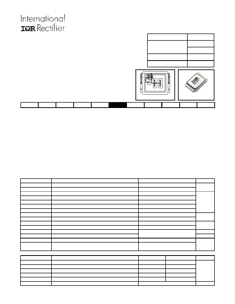
AUTOMOTIVE GRADE
DirectFET ISOMETRIC
M4
HEXFET is a registered trademark of International Rectifier.
SB
SC
M2
M4
L4
L6
L8
DD
G
S
SS
S
V(BR)DSS
60V
RDS(on) typ.
5.5m
max.
7.0m
ID (Silicon Limited)
68A
Qg
35nC
11/08/10
AUIRF7648M2TR
AUIRF7648M2TR1
Advanced Process Technology
Optimized for Automotive Motor Drive, DC-DC and
other Heavy Load Applications
Exceptionally Small Footprint and Low Profile
High Power Density
Low Parasitic Parameters
Dual Sided Cooling
175°C Operating Temperature
Repetitive Avalanche Capability for Robustness and
Reliability
Lead Free, RoHS Compliant and Halogen Free
Automotive Qualified *
Absolute Maximum Ratings
Stresses beyond those listed under “Absolute Maximum Ratings” may cause permanent damage to the device. These are stress ratings only; and
functional operation of the device at these or any other condition beyond those indicated in the specifications is not implied.Exposure to absolute-
maximum-rated conditions for extended periods may affect device reliability. The thermal resistance and power dissipation ratings are measured
under board mounted and still air conditions. Ambient temperature (TA) is 25°C, unless otherwise specified.
Parameter
Units
VDS
Drain-to-Source Voltage
VGS
Gate-to-Source Voltage
ID @ TC = 25°C
Continuous Drain Current, VGS @ 10V (Silicon Limited)f
ID @ TC = 100°C
Continuous Drain Current, VGS @ 10V (Silicon Limited)f
ID @ TA = 25°C
Continuous Drain Current, VGS @ 10V (Silicon Limited)e
ID @ TC = 25°C
Continuous Drain Current, VGS @ 10V (Package Limited)
IDM
Pulsed Drain Current
g
PD @TC = 25°C
Power Dissipation
f
PD @TA = 25°C
Power Dissipation
e
EAS
Single Pulse Avalanche Energy (Thermally Limited)
h
EAS (tested)
Single Pulse Avalanche Energy Tested Value
h
IAR
Avalanche Current
g
A
EAR
Repetitive Avalanche Energy
g
mJ
TP
Peak Soldering Temperature
TJ
Operating Junction and
TSTG
Storage Temperature Range
Thermal Resistance
Parameter
Typ.
Max.
Units
RθJA
Junction-to-Ambient
e
–––
60
RθJA
Junction-to-Ambient
j
12.5
–––
RθJA
Junction-to-Ambient
k
20
–––
RθJ-Can
Junction-to-Can
fl
–––
2.4
RθJ-PCB
Junction-to-PCB Mounted
1.0
–––
Linear Derating Factor
f
W/°C
291
°C/W
0.42
70
°C
-55 to + 175
See Fig. 18a,18b,16,17
mJ
270
Max.
68
48
272
± 20
179
14
60
2.5
V
A
W
63
PD - 96317B
相關(guān)PDF資料 |
PDF描述 |
|---|---|
| AUIRF7665S2TR1 | 4.1 A, 100 V, 0.062 ohm, N-CHANNEL, Si, POWER, MOSFET |
| AUIRF7665S2TR | 4.1 A, 100 V, 0.062 ohm, N-CHANNEL, Si, POWER, MOSFET |
| AUIRF7665S2TR | 4.1 A, 100 V, 0.062 ohm, N-CHANNEL, Si, POWER, MOSFET |
| AUIRF7665S2TR1 | 4.1 A, 100 V, 0.062 ohm, N-CHANNEL, Si, POWER, MOSFET |
| AUIRF7675M2TR1 | 4.4 A, 150 V, 0.056 ohm, N-CHANNEL, Si, POWER, MOSFET |
相關(guān)代理商/技術(shù)參數(shù) |
參數(shù)描述 |
|---|---|
| AUIRF7665S2TR | 功能描述:MOSFET 100V AUTO GRADE 1 N-CH HEXFET RoHS:否 制造商:STMicroelectronics 晶體管極性:N-Channel 汲極/源極擊穿電壓:650 V 閘/源擊穿電壓:25 V 漏極連續(xù)電流:130 A 電阻汲極/源極 RDS(導(dǎo)通):0.014 Ohms 配置:Single 最大工作溫度: 安裝風(fēng)格:Through Hole 封裝 / 箱體:Max247 封裝:Tube |
| AUIRF7665S2TR1 | 功能描述:MOSFET 100V AUTO GRADE 1 N-CH HEXFET RoHS:否 制造商:STMicroelectronics 晶體管極性:N-Channel 汲極/源極擊穿電壓:650 V 閘/源擊穿電壓:25 V 漏極連續(xù)電流:130 A 電阻汲極/源極 RDS(導(dǎo)通):0.014 Ohms 配置:Single 最大工作溫度: 安裝風(fēng)格:Through Hole 封裝 / 箱體:Max247 封裝:Tube |
| AUIRF7669L2TR | 功能描述:MOSFET 100V AUTO GRADE 1 N-CH HEXFET RoHS:否 制造商:STMicroelectronics 晶體管極性:N-Channel 汲極/源極擊穿電壓:650 V 閘/源擊穿電壓:25 V 漏極連續(xù)電流:130 A 電阻汲極/源極 RDS(導(dǎo)通):0.014 Ohms 配置:Single 最大工作溫度: 安裝風(fēng)格:Through Hole 封裝 / 箱體:Max247 封裝:Tube |
| AUIRF7669L2TR 1 | 制造商:International Rectifier 功能描述:AUIRF7669L2TR1 - MOSFET,,N CH,100V,375A,DIRECTFET,L8 |
| AUIRF7669L2TR1 | 功能描述:MOSFET 100V AUTO GRADE 1 N-CH HEXFET RoHS:否 制造商:STMicroelectronics 晶體管極性:N-Channel 汲極/源極擊穿電壓:650 V 閘/源擊穿電壓:25 V 漏極連續(xù)電流:130 A 電阻汲極/源極 RDS(導(dǎo)通):0.014 Ohms 配置:Single 最大工作溫度: 安裝風(fēng)格:Through Hole 封裝 / 箱體:Max247 封裝:Tube |
發(fā)布緊急采購(gòu),3分鐘左右您將得到回復(fù)。