- 您現(xiàn)在的位置:買賣IC網(wǎng) > PDF目錄42904 > ATF-54143-TR1G (AGILENT TECHNOLOGIES INC) C BAND, GaAs, N-CHANNEL, RF SMALL SIGNAL, HEMFET PDF資料下載
參數(shù)資料
| 型號: | ATF-54143-TR1G |
| 廠商: | AGILENT TECHNOLOGIES INC |
| 元件分類: | 小信號晶體管 |
| 英文描述: | C BAND, GaAs, N-CHANNEL, RF SMALL SIGNAL, HEMFET |
| 封裝: | PLASTIC, SC-70, 4 PIN |
| 文件頁數(shù): | 14/17頁 |
| 文件大?。?/td> | 212K |
| 代理商: | ATF-54143-TR1G |
6
ATF-54143 Typical Scattering Parameters,
VDS = 3V, IDS = 40 mA
Freq.
S11
S21
S12
S22
MSG/MAG
GHz
Mag.
Ang.
dB
Mag.
Ang.
Mag.
Ang.
Mag.
Ang.
dB
0.1
0.99
-17.6
27.99
25.09
168.5
0.009
80.2
0.59
-12.8
34.45
0.5
0.83
-76.9
25.47
18.77
130.1
0.036
52.4
0.44
-54.6
27.17
0.9
0.72
-114
22.52
13.37
108
0.047
40.4
0.33
-78.7
24.54
1.0
0.70
-120.6
21.86
12.39
103.9
0.049
38.7
0.31
-83.2
24.03
1.5
0.65
-146.5
19.09
9.01
87.4
0.057
33.3
0.24
-99.5
21.99
1.9
0.63
-162.1
17.38
7.40
76.6
0.063
30.4
0.20
-108.6
20.70
2.0
0.62
-165.6
17.00
7.08
74.2
0.065
29.8
0.19
-110.9
20.37
2.5
0.61
178.5
15.33
5.84
62.6
0.072
26.6
0.15
-122.6
19.09
3.0
0.61
164.2
13.91
4.96
51.5
0.080
22.9
0.12
-137.5
17.92
4.0
0.63
138.4
11.59
3.80
31
0.094
14
0.10
176.5
15.33
5.0
0.66
116.5
9.65
3.04
11.6
0.106
4.2
0.14
138.4
12.99
6.0
0.69
97.9
8.01
2.51
-6.7
0.118
-6.1
0.17
117.6
11.50
7.0
0.71
80.8
6.64
2.15
-24.5
0.128
-17.6
0.20
98.6
10.24
8.0
0.72
62.6
5.38
1.86
-42.5
0.134
-29.3
0.22
73.4
8.83
9.0
0.76
45.2
4.20
1.62
-60.8
0.145
-40.6
0.27
52.8
8.17
10.0
0.83
28.2
2.84
1.39
-79.8
0.150
-56.1
0.37
38.3
8.57
11.0
0.85
13.9
1.42
1.18
-96.9
0.149
-69.3
0.45
25.8
7.47
12.0
0.88
-0.5
0.23
1.03
-112.4
0.150
-81.6
0.51
12.7
7.50
13.0
0.89
-15.1
-0.86
0.91
-129.7
0.149
-95.7
0.54
-4.1
6.60
14.0
0.87
-31.6
-2.18
0.78
-148
0.143
-110.3
0.61
-20.1
4.57
15.0
0.88
-46.1
-3.85
0.64
-164.8
0.132
-124
0.65
-34.9
3.47
16.0
0.87
-54.8
-5.61
0.52
-178.4
0.121
-134.6
0.70
-45.6
2.04
17.0
0.87
-62.8
-7.09
0.44
170.1
0.116
-144.1
0.73
-55.9
1.05
18.0
0.92
-73.6
-8.34
0.38
156.1
0.109
-157.4
0.76
-68.7
1.90
Freq
Fmin
Γopt
Rn/50
Ga
GHz
dB
Mag.
Ang.
dB
0.5
0.17
0.34
34.80
0.04
27.83
0.9
0.22
0.32
53.00
0.04
23.57
1.0
0.24
0.32
60.50
0.04
22.93
1.9
0.42
0.29
108.10
0.04
18.35
2.0
0.45
0.29
111.10
0.04
17.91
2.4
0.51
0.30
136.00
0.04
16.39
3.0
0.59
0.32
169.90
0.05
15.40
3.9
0.69
0.34
-151.60
0.05
13.26
5.0
0.90
0.45
-119.50
0.09
11.89
5.8
1.14
0.50
-101.60
0.16
10.95
6.0
1.17
0.52
-99.60
0.18
10.64
7.0
1.24
0.58
-79.50
0.33
9.61
8.0
1.57
0.60
-57.90
0.56
8.36
9.0
1.64
0.69
-39.70
0.87
7.77
10.0
1.8
0.80
-22.20
1.34
7.68
Notes:
1. F
min values at 2 GHz and higher are based on measurements while the Fmins below 2 GHz have been extrapolated. The Fmin values are based on a set of
16 noise figure measurements made at 16 different impedances using an ATN NP5 test system. From these measurements a true Fmin is calculated.
Refer to the noise parameter application section for more information.
2. S and noise parameters are measured on a microstrip line made on 0.025 inch thick alumina carrier. The input reference plane is at the end of the gate
lead. The output reference plane is at the end of the drain lead. The parameters include the effect of four plated through via holes connecting source
landing pads on top of the test carrier to the microstrip ground plane on the bottom side of the carrier. Two 0.020 inch diameter via holes are placed
within 0.010 inch from each source lead contact point, one via on each side of that point.
Typical Noise Parameters,
VDS = 3V, IDS = 40 mA
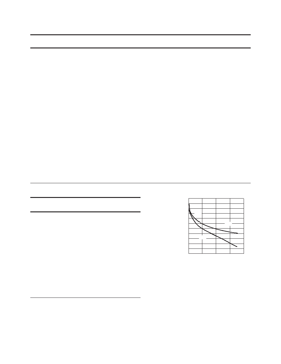
Figure 19. MSG/MAG and |S21|
2 vs.
Frequency at 3V, 40 mA.
MAG
S21
FREQUENCY (GHz)
MSG/MAG
and
S
21
(dB)
020
10
515
40
35
30
25
20
15
10
5
0
-5
10
-15
MSG
相關PDF資料 |
PDF描述 |
|---|---|
| ATF-54143-TR2 | C BAND, GaAs, N-CHANNEL, RF SMALL SIGNAL, HEMFET |
| ATF-54143-TR2G | C BAND, GaAs, N-CHANNEL, RF SMALL SIGNAL, HEMFET |
| ATF-541M4-TR1G | X BAND, Si, N-CHANNEL, RF SMALL SIGNAL, HEMFET |
| ATF-541M4-TR2G | X BAND, Si, N-CHANNEL, RF SMALL SIGNAL, HEMFET |
| ATF-541M4-BLK | X BAND, Si, N-CHANNEL, RF SMALL SIGNAL, HEMFET |
相關代理商/技術參數(shù) |
參數(shù)描述 |
|---|---|
| ATF-54143-TR2 | 制造商:AGILENT 制造商全稱:AGILENT 功能描述:Low Noise Enhancement Mode Pseudomorphic HEMT in a Surface Mount Plastic Package |
| ATF-54143-TR2G | 功能描述:射頻GaAs晶體管 Transistor GaAs Single Voltage RoHS:否 制造商:TriQuint Semiconductor 技術類型:pHEMT 頻率:500 MHz to 3 GHz 增益:10 dB 噪聲系數(shù): 正向跨導 gFS(最大值/最小值):4 S 漏源電壓 VDS: 閘/源擊穿電壓:- 8 V 漏極連續(xù)電流:3 A 最大工作溫度:+ 150 C 功率耗散:10 W 安裝風格: 封裝 / 箱體: |
| ATF-541M4 | 制造商:AGILENT 制造商全稱:AGILENT 功能描述:Low Noise Enhancement Mode Pseudomorphic HEMT in a Miniature Leadless Package |
| ATF-541M4-BLK | 功能描述:射頻GaAs晶體管 Transistor GaAs Single Voltage RoHS:否 制造商:TriQuint Semiconductor 技術類型:pHEMT 頻率:500 MHz to 3 GHz 增益:10 dB 噪聲系數(shù): 正向跨導 gFS(最大值/最小值):4 S 漏源電壓 VDS: 閘/源擊穿電壓:- 8 V 漏極連續(xù)電流:3 A 最大工作溫度:+ 150 C 功率耗散:10 W 安裝風格: 封裝 / 箱體: |
| ATF-541M4-BLK | 制造商:Avago Technologies 功能描述:RF BIPOLAR TRANSISTOR |
發(fā)布緊急采購,3分鐘左右您將得到回復。