- 您現(xiàn)在的位置:買賣IC網(wǎng) > PDF目錄378405 > AND8098 (ON SEMICONDUCTOR) Low-Cost 100 mA High-Voltage Buck and Buck-Boost Using NCP1052 PDF資料下載
參數(shù)資料
| 型號(hào): | AND8098 |
| 廠商: | ON SEMICONDUCTOR |
| 英文描述: | Low-Cost 100 mA High-Voltage Buck and Buck-Boost Using NCP1052 |
| 中文描述: | 低成本百毫安高電壓降壓和降壓升壓使用NCP1052 |
| 文件頁數(shù): | 6/10頁 |
| 文件大小: | 93K |
| 代理商: | AND8098 |
AND8098/D
http://onsemi.com
6
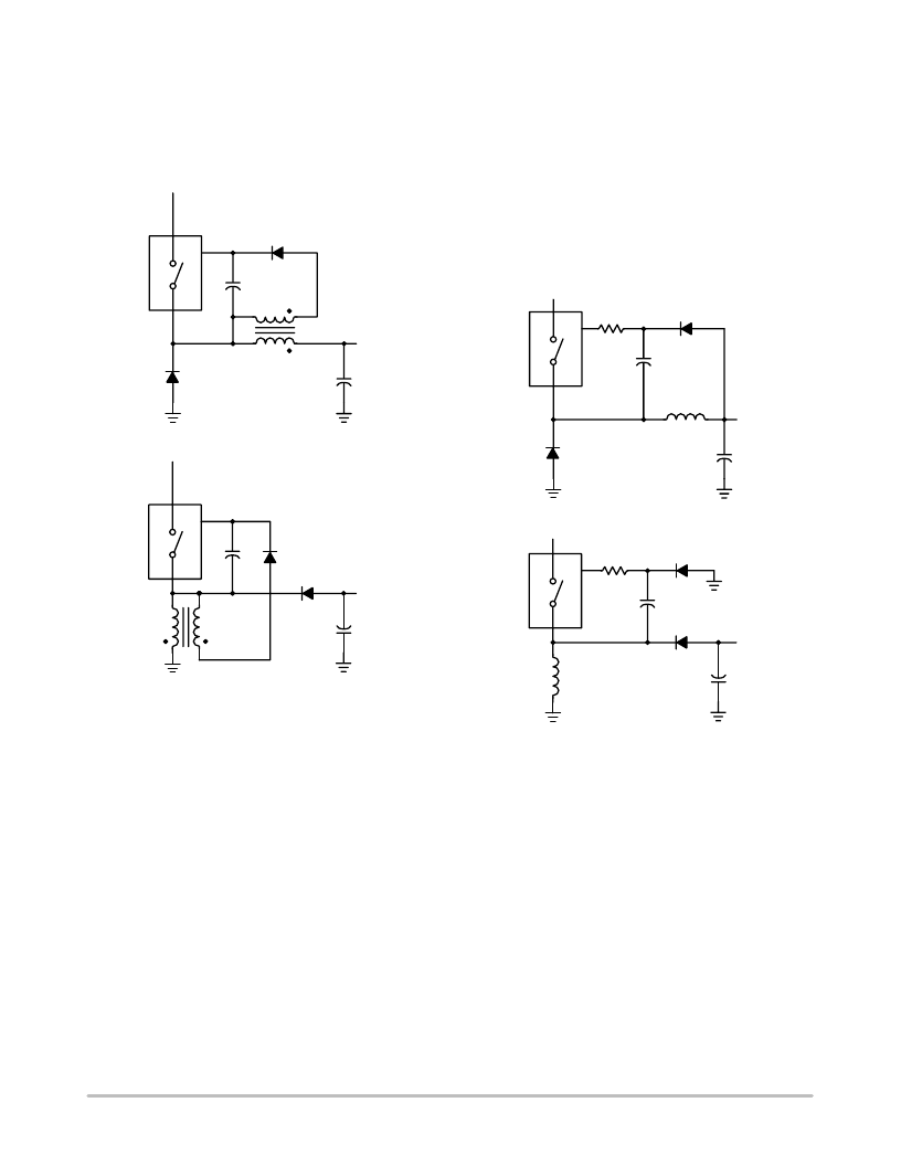
The proposed buck-boost is better in term of the standby
ability. It is because the V
CC
charging current in Figure 2(b)
only passes through the inductor. The charging current
pulses become an averaged energy stored in the inductor and
consume smaller amount of power comparing to the buck
case.
Figure 7. Auxiliary Winding to improve standby
Abillity
(a) Buck
(b) Buck-boost
The auxiliary winding to supply the V
CC
voltage in Figure
7 is a method to improve the standby ability. The auxiliary
winding keeps the V
CC
voltage above 7.5 V and disable the
V
CC
charging current and hence its standby loss. The
auxiliary winding is coupled from the inductor L with
polarity same as the regulated output voltage. The V
CC
voltage in the auxiliary winding is designed to be between
the normal V
CC
limits of 7.5 and 8.5 V typically. The
frequency jittering feature loses when the V
CC
voltage is
fixed. When output is shorted, there will be no voltage
coming from the auxiliary winding and the circuit will enter
fault mode with the 4.5 V-8.5 V-7.5 V-4.5 V hysteresis
loop.
Another method to supply the V
CC
voltage is coupling
capacitor technique in Figure 8. The output voltage is
coupled to the inserted capacitor when the diodes are closed.
The voltage drop of the diodes compensate each other.
Hence, the diode voltage drop effect can be neglected. The
NCP1052 needs a nominal V
CC
voltage of 8V. The inserted
resistor consumes some voltage from the output voltage V
out
to make a 8V to the V
CC
pin. Based on the 0.5mA typical
current consumption of V
CC
pin. The inserted resistance
value is (V
out
- 8) / 0.5 k .
Figure 8. Coupling Capacitor Technique to
Improve Standby Abillity
(a) Buck
(b) Buck-boost
Temperature Rise
The NCP1052 is a very compact package with the control
circuit and high-voltage power switch. Its typical on
resistance is 22
. Temperature rise exists. It is
recommended to design the PCB board with a large copper
area next to the device as a heatsink. This heatsink decreases
相關(guān)PDF資料 |
PDF描述 |
|---|---|
| AND8099 | 5.0 V, 2.0 A Flyback Converter |
| AND8109 | LED CONSTANT CURRENT SOURCE SCHEME |
| AND8112 | A Quasi-Resonant SPICE Model Eases Feedback Loop Designs |
| AND8116 | Integrated Relay/Inductive Load Drivers for Industrial and Automotive Applications |
| AND8116D | Integrated Relay/Inductive Load Drivers for Industrial and Automotive Applications |
相關(guān)代理商/技術(shù)參數(shù) |
參數(shù)描述 |
|---|---|
| AND8099 | 制造商:ONSEMI 制造商全稱:ON Semiconductor 功能描述:5.0 V, 2.0 A Flyback Converter |
| AND8099/D | 制造商:ONSEMI 制造商全稱:ON Semiconductor 功能描述:5.0 V, 2.0 A Flyback Converter |
| AND8104/D | 制造商:未知廠家 制造商全稱:未知廠家 功能描述:MicroIntegration Technology Solutions for Protection in High Speed I/O Data Lines |
| AND8109 | 制造商:ONSEMI 制造商全稱:ON Semiconductor 功能描述:LED CONSTANT CURRENT SOURCE SCHEME |
| AND8112 | 制造商:ONSEMI 制造商全稱:ON Semiconductor 功能描述:A Quasi-Resonant SPICE Model Eases Feedback Loop Designs |
發(fā)布緊急采購,3分鐘左右您將得到回復(fù)。