- 您現(xiàn)在的位置:買賣IC網 > PDF目錄378403 > AN1042D (ON SEMICONDUCTOR) High Fidelity Switching Audio Amplifiers Using TMOS Power MOSFETs PDF資料下載
參數(shù)資料
| 型號: | AN1042D |
| 廠商: | ON SEMICONDUCTOR |
| 英文描述: | High Fidelity Switching Audio Amplifiers Using TMOS Power MOSFETs |
| 中文描述: | 高保真開關音頻放大器使用的TMOS功率MOSFET |
| 文件頁數(shù): | 3/12頁 |
| 文件大小: | 108K |
| 代理商: | AN1042D |
AN1042/D
http://onsemi.com
3
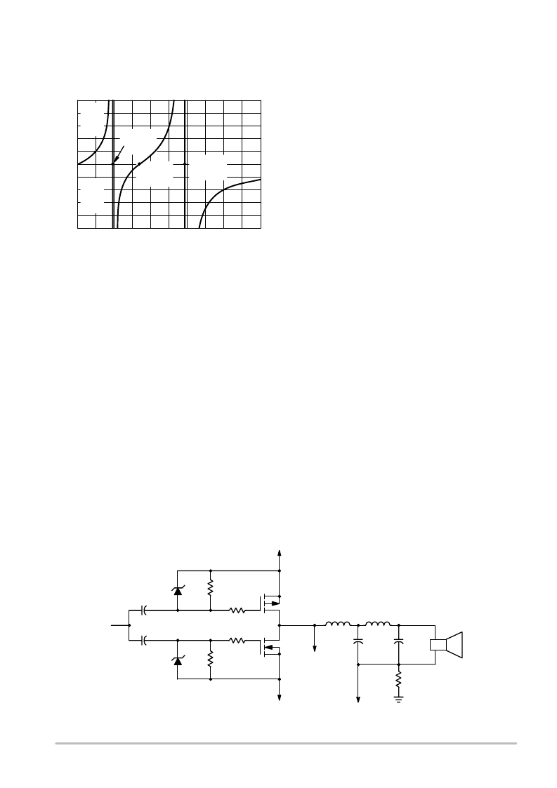
Figure 4. Four Pole Butterworth Filter
Output Impedance
4
5
3
0
2
1
N
I
R
0
12
24
36
48
60
kHz
–5
–4
–3
–2
–1
N
C
R
Parallel
Resonance
11.4 kHz
Series
Resonance
20 kHz
Parallel
Resonance
35.2 kHz
The amplifier output impedance at dc is about 4
milliohms and gradually becomes inductive. At 100 Hz, its
output impedance is 0.1 ohm giving a damping factor of 80.
Damping factor is the ratio of load impedance to amplifier
output impedance.
The complementary power MOSFET output stage of the
amplifier is shown in Figure 5. It generates a
±
44 volt
square wave whose duty cycle can vary from 5% to 95%.
This variable duty cycle square wave is fed to the output
filter where the low frequency component is passed on to
the 8 ohm speaker. This filter allows frequencies under
20 kHz to pass with negligible loss, but greatly attenuates
the switching frequency. Since both sources are connected
to a supply rail, a drive of 10 volts peak to peak on each gate
insures full turn on. A buffer amp using
±
5 volts supplies
provides this drive.
The 4.7 ohm resistors, R17 and R18, in each gate lead
prevents high frequency oscillation during switching. The 12
volt Zeners, CR3 and CR4, serve both as conventional
diode clamps and provide static discharge protection. They
act as dc restorers, and are made necessary by the ac
coupling. The 10 k resistors, R15 and R16, provide a slight
discharge path to keep conduction pulses in the clamp
diodes. They also discharge the gates in about 1
millisecond if the drive signal is lost. About 9 volts of
turn–on bias is applied to each gate. Tight coupling
between the gates prevents simultaneous turn–on of both
devices.
The output stage inverts the drive signal and generates
rise and fall times of about 30 nanoseconds. It is designed
to put out a maximum current of
±
5 amps down to a
frequency of 0.1 Hertz. Below that frequency, maximum
current may need to be derated to prevent alternate
overheating of each output device. Excessive heatsink
temperature increases the ON resistance and the storage
time of the source drain diode. The resultant increase in
losses can lead to thermal runaway.
The drive waveform duty cycle must be a linear function
of the control voltage. The Duty Cycle Controller is shown
in Figure 6. A square wave of
±
5 volts at 120 kHz is coupled
through C1 and R1 to integrator U1B. C1 blocks dc and R1
is the integrator resistor. C2 is the integrator capacitor
which generates a
±
2 volt triangle on the output of U1B. R2
provides a small amount of dc leakage to insure that the
output has no significant dc component. R3 couples the
triangle to the noninverting input of comparator U1D. It
improves the waveform by isolating the input capacitance
of the comparator from the integrator. The dc offset on the
triangle is equal to the offset of U1B and its linearity is
better than 1%.
Input audio is applied to the inverting input of U2C
through R4. The output square wave of the power amp is
applied through R5 to the same summing point. U2C
functions as an integrator with C3 as the integrator
capacitor. Since R5 is 20 times R4, an inverting voltage
gain of 20 must result if the input of U2C is to be at ground.
The output of U2C serves as the error voltage and is fed to
the inverting input of U1D through R6 and R7. C4
eliminates short spikes on the error buss. Current limiting
circuitry is connected to the junction of R6 and R7. When
current drawn from the amplifier tries to exceed safe limits,
the error voltage is overridden and overcurrent is prevented.
R27
8
Speaker
Figure 5. Output Circuit of a Class D Amplifier
C10
C9
Current Sense
L2
L1
Feedback
+44
R17
R18
R15
R16
CR3
CR4
C7
C8
Drive
Q3
Q4
相關PDF資料 |
PDF描述 |
|---|---|
| AN1062 | Circular Connector; No. of Contacts:6; Series:MS27508; Body Material:Aluminum; Connecting Termination:Crimp; Connector Shell Size:8; Circular Contact Gender:Socket; Circular Shell Style:Box Mount Receptacle; Insert Arrangement:8-35 RoHS Compliant: No |
| AN1077 | ISL6244EVAL1 Multi-phase Evaluation Board Setup Procedure |
| AN1082 | Using the ISL6401 RSLIC PWM Controller Evaluation Board |
| AN1406 | DESIGNING WITH PECL (ECL AT + 5.0) |
| AN1504 | Metastability and the ECLinPS Family |
相關代理商/技術參數(shù) |
參數(shù)描述 |
|---|---|
| AN1043 | 制造商:MICROCHIP 制造商全稱:Microchip Technology 功能描述:Unique Features of the MCP23X08/17 GPIO Expanders |
| AN-1043 | 制造商:CYMBET 制造商全稱:CYMBET 功能描述:EnerChip CC as Backup Power for a DS1390 Real-Time Clock |
| AN10436 | 制造商:PHILIPS 制造商全稱:NXP Semiconductors 功能描述:TDA8932B/33(B) Class-D audio amplifier |
| AN1045 | 制造商:STMICROELECTRONICS 制造商全稱:STMicroelectronics 功能描述:ST7 S/W IMPLEMENTATION OF I2C BUS MASTER |
| AN-1045 | 制造商:CYMBET 制造商全稱:CYMBET 功能描述:EnerChip CC Backup Power for Micro Crystal RV-2123 RTC |
發(fā)布緊急采購,3分鐘左右您將得到回復。