- 您現(xiàn)在的位置:買賣IC網(wǎng) > PDF目錄378403 > AN013 (Intersil Corporation) JT 128C 128#22D SKT RECP PDF資料下載
參數(shù)資料
| 型號(hào): | AN013 |
| 廠商: | Intersil Corporation |
| 英文描述: | JT 128C 128#22D SKT RECP |
| 中文描述: | 人們始終想關(guān)于ICL8038知情權(quán) |
| 文件頁數(shù): | 3/4頁 |
| 文件大小: | 87K |
| 代理商: | AN013 |
3
Question 10
Your data sheet is very confusing about the phase relationship
of the various waveforms.
Answer
Sorry about that! The thing to remember is that the triangle
and sine wave must be in phase since one is derived from
the other. A check on the way the circuit works shows that
the pulse waveform on pin 9 will be high as the capacitor
charges (positive slope on the triangle wave) and will be low
during discharge (negative slope on the triangle wave).
The latest data sheet corrects the photograph Figure 7 on Page
5 of the data sheet. The 20% duty cycle square wave was
inverted, i.e., should be 80% duty cycle. Also, on that page
under “Waveform Timing” the related sentences should read
“R
A
controls the rising portion of the triangle and sine-wave and
the 1 state of the square wave.” Also, “the falling portion of the
triangle and sine wave and the 0 state of the square wave is:”
Question 11
Under Parameter Test Conditions on Page 3 of your 8038
data sheet, the suggested value for Min and Max duty cycle
adjust don’t seem to work.
Answer
The positive charging current is determined by R
A
alone
since the current from R
B
is switched off. (See 8038 Applica-
tion Note AN012 for complete circuit description.) The nega-
tive discharge current is the
difference
between the R
A
current and twice the R
B
current. Therefore, changing R
B
will affect only the discharge time, while changing R
A
will
affect both charge and discharge times. For short negative
going pulses (greater than 50% duty cycle) we can lower the
value of R
B
(e.g., R
A
= 50k
and R
B
= 1.6k
). For short
positive going pulses (duty cycles less than 50%) the limiting
values are reached when the current in R
A
is twice that in
R
B
(e.g., R
B
= 50k
). This has been corrected on the latest
data sheet.
Question 12
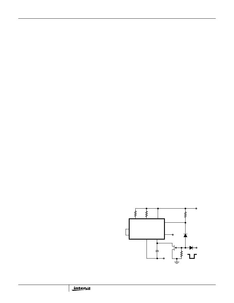
I need to switch the waveforms off and on. What’s a good
way to strobe the 8038
Answer
With a dual supply voltage (e.g.,
±
15V) the external capaci-
tor (pin 10) can be shorted to ground so that the sine wave
and triangle wave always begin at a zero crossing point.
Random switching has a 50/50 chance of starting on a posi-
tive or negative slope. A simple AND gate using pin 9 will
allow the strobe to act only on one slope or the other, see
Figure 2. Using only a single supply, the capacitor (pin 10)
can be switched either to V+ or ground to force the compara-
tor to set in either the charge or discharge mode. The disad-
vantage of this technique is that the beginning cycle of the
next burst will be 30% longer than the normal cycle.
Question 13
How can I buffer the sine wave output without loading it down
Answer
The simplest circuit is a simple op amp follower as shown in Fig-
ure 3A. Another circuit shown in Figure 3B allows amplitude and
offset controls without disturbing the 8038. Either circuit can be
DC or AC coupled. For AC coupling the op amp non-inverting
input must be returned to ground with a 100k
resistor.
Question 14
Your 8038 data sheet implies that all waveforms can operate up
to 1MHz. Is this true
Answer
Unfortunately, only the square wave output is useful at that
frequency. As can be seen from the curves on page 4 of the
data sheet, distortion on the sine wave and linearity of the tri-
angle wave fall off rapidly above 200kHz.
Question 15
Is it normal for this device to run hot to the touch
Answer
Yes. The 8038 is essentially resistive. The power dissipation
is then E
2
/R and at
±
15V, the device does run hot. Extensive
life testing under this operating condition and maximum
ambient temperature has verified the reliability of this prod-
uct.
Question 16
How stable are the output amplitudes versus temperature
Answer
The amplitude of the triangle waveform decreases slightly
with temperature. The typical amplitude coefficient is
-0.01%/
o
C, giving a drop of about 1% at 125
o
C. The sine
output is less sensitive and decreases only about 0.6% at
125
o
C. For the square wave output the V
CE(SAT)
goes from
0.12V at 25
o
C to 0.17V at 125
o
C. Leakage current in the “1”
state is less than a few nanoamperes even at 125
o
C and is
usually negligible.
FIGURE 2. STROBE-TONE BURST GENERATOR
2N4392
R
A
R
B
15K
+15V
-15V
STROBE
1N914
OFF
ON
100K
C
1N914
8038
+15V (>0V)
-15V (< -10V)
2
4
5
6
7
8
9
10
11
Application Note 013
相關(guān)PDF資料 |
PDF描述 |
|---|---|
| AN1025 | Converting A 5.0V Supply Rail To A Regulated 3.0V |
| AN1034 | Analog Switch and Multiplexer Applications |
| AN1042 | High Fidelity Switching Audio Amplifiers Using TMOS Power MOSFETs |
| AN1042D | High Fidelity Switching Audio Amplifiers Using TMOS Power MOSFETs |
| AN1062 | Circular Connector; No. of Contacts:6; Series:MS27508; Body Material:Aluminum; Connecting Termination:Crimp; Connector Shell Size:8; Circular Contact Gender:Socket; Circular Shell Style:Box Mount Receptacle; Insert Arrangement:8-35 RoHS Compliant: No |
相關(guān)代理商/技術(shù)參數(shù) |
參數(shù)描述 |
|---|---|
| AN0130 | 制造商:SUPERTEX 制造商全稱:SUPERTEX 功能描述:8 Channel Power MOSFET Array Monolithic N-channel Enchancement Mode |
| AN0130NA | 制造商:SUPERTEX 制造商全稱:SUPERTEX 功能描述:8 Channel Power MOSFET Array Monolithic N-channel Enchancement Mode |
| AN0130NB | 制造商:SUPERTEX 制造商全稱:SUPERTEX 功能描述:8 Channel Power MOSFET Array Monolithic N-channel Enchancement Mode |
| AN0130ND | 制造商:SUPERTEX 制造商全稱:SUPERTEX 功能描述:8 Channel Power MOSFET Array Monolithic N-channel Enchancement Mode |
| AN0132 | 制造商:SUPERTEX 制造商全稱:SUPERTEX 功能描述:8 Channel Power MOSFET Array Monolithic N-channel Enchancement Mode |
發(fā)布緊急采購,3分鐘左右您將得到回復(fù)。