- 您現(xiàn)在的位置:買賣IC網(wǎng) > PDF目錄378403 > AN-242 (National Semiconductor Corporation) LJT 18C 18#20 SKT RECP PDF資料下載
參數(shù)資料
| 型號: | AN-242 |
| 廠商: | National Semiconductor Corporation |
| 英文描述: | LJT 18C 18#20 SKT RECP |
| 中文描述: | 應(yīng)用新的精密運算放大器 |
| 文件頁數(shù): | 5/16頁 |
| 文件大小: | 267K |
| 代理商: | AN-242 |
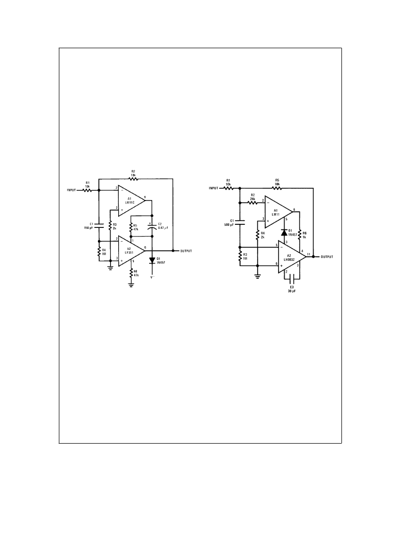
An optimized circuit for the inverting amplifier connection is
shown inFigure 8. The LM11 is DC coupled to the input and
drives the balance terminals of the fast amplifier. The fast
amplifier is AC coupled to the input and drives the output.
This isolates FET leakage from the input circuitry.
As can be seen, the method of coupling into the balance
terminals will vary depending on the internal configuration of
the fast amplifier. If the quiescent voltage on the balance
terminals is beyond the output swing of the LM11, a differ-
ential coupling must be used, as inFigure 8a. A lead capaci-
tor, C2, reduces the AC swing required at the LM11 output.
The clamp diode, D1, insures that the LM11 does not over-
drive the fast amplifier in slew.
If the quiescent voltage on the balance terminals is such
that the LM11 can drive directly, the circuit inFigure 8b can
be used. A clamp diode from the other balance terminal to
internal circuitry of the LM11 keeps the output from swing-
ing too far from the null value, and a resistor may be re-
quired in series with its output to insure stability.
Measurements indicate that the slew rate of the fast amplifi-
er is unimpaired, as is the settling time to 1 mV for a 20V
output excursion. If the composite amplifier is overdriven so
that the output saturates, there will be an added recovery
delay because the coupling capacitor to the fast amplifier
takes on a charge with the summing node off ground.
Therefore, C1 should be made as small as possible. But
going below the values given may introduce gain error.
If the bias current of the fast amplifier meets circuit require-
ments, it can be direct-coupled to the input. In this case,
offset voltage is improved, not bias current. But overload
recovery can be reduced. The AC coupling to the fast-ampli-
fier input might best be eliminated for limited-temperature-
range operation.
This connection also increases the open-loop gain beyond
that of the LM11, particularly since two-pole compensation
can be effected to reduce AC gain error at moderate fre-
quencies. The DC gains measured showed something in
excess of 140 dB.
TL/H/7479–9
a. with standard BI-FET
TL/H/7479–10
b. with fast hybrid
Figure 8. These inverters have bias current and offset voltage of LM11 along with speed of the FET op amps. Open
loop gain is about 140 dB and settling time to 1 mV about 8
m
s. Excess overload-recovery delay can be
eliminated by directly coupling the FET amplifier to summing node.
5
相關(guān)PDF資料 |
PDF描述 |
|---|---|
| AN-40 | Application Note 40 |
| AN-5002 | LJT 18C 18#20 SKT WALL RECP |
| AN-5025 | Applications Using the GTLP10B320 |
| AN-5026 | Circular Connector; No. of Contacts:19; Series:MS27656; Body Material:Aluminum; Connecting Termination:Crimp; Connector Shell Size:15; Circular Contact Gender:Pin; Circular Shell Style:Wall Mount Receptacle; Insert Arrangement:15-19 RoHS Compliant: No |
| AN-5031 | GTLP Power Configuration |
相關(guān)代理商/技術(shù)參數(shù) |
參數(shù)描述 |
|---|---|
| AN24-22 | 制造商:AN# - MILITARY 功能描述: |
| AN24-31A | 制造商:AN# - MILITARY 功能描述: |
| AN2440 | 制造商:Distributed By MCM 功能描述:USB to DVI Adapter |
| AN2441S | 制造商:未知廠家 制造商全稱:未知廠家 功能描述:Color Encoder Circuit |
| AN245 | 制造商:Panasonic Industrial Company 功能描述:IC |
發(fā)布緊急采購,3分鐘左右您將得到回復(fù)。