- 您現(xiàn)在的位置:買(mǎi)賣(mài)IC網(wǎng) > PDF目錄362278 > AM52-0001 1.2 W High Efficiency Power Amplifier 800 - 960 MHz PDF資料下載
參數(shù)資料
| 型號(hào): | AM52-0001 |
| 英文描述: | 1.2 W High Efficiency Power Amplifier 800 - 960 MHz |
| 中文描述: | 1.2 W高效率數(shù)字功放800 - 960兆赫 |
| 文件頁(yè)數(shù): | 2/6頁(yè) |
| 文件大小: | 79K |
| 代理商: | AM52-0001 |
1.2 W High Efficiency Power Amplifier
AM52-0001
V1.00
Specifications Subject to Change Without Notice.
2
North America: Tel. (800) 366-2266
Asia/Pacific: Tel. +81 3 3226-8761
Europe:
Fax (800) 618-8883 Fax +81 3 3226-8769
M/A-COM Inc.
Tel. +44 (1344) 869-595
Fax +44 (1344) 300 020
Absolute Maximum Ratings
1
Parameter
Absolute Maximum
+23 dBm
V
DD
= + 10 Volts
V
GG
= - 6 Volts
+150
°
C
-65
°
C to +150
°
C
-40
°
C to +85
°
C
Input Power
2
Operating Voltage
2
Junction Temperature
3
Storage Temperature
Operating Temperature
1. Exceeding any one or combination of these limits may cause
permanent damage.
2. Ambient Temperature (T
A
) = + 25
°
C
3. See temperature derating curve.
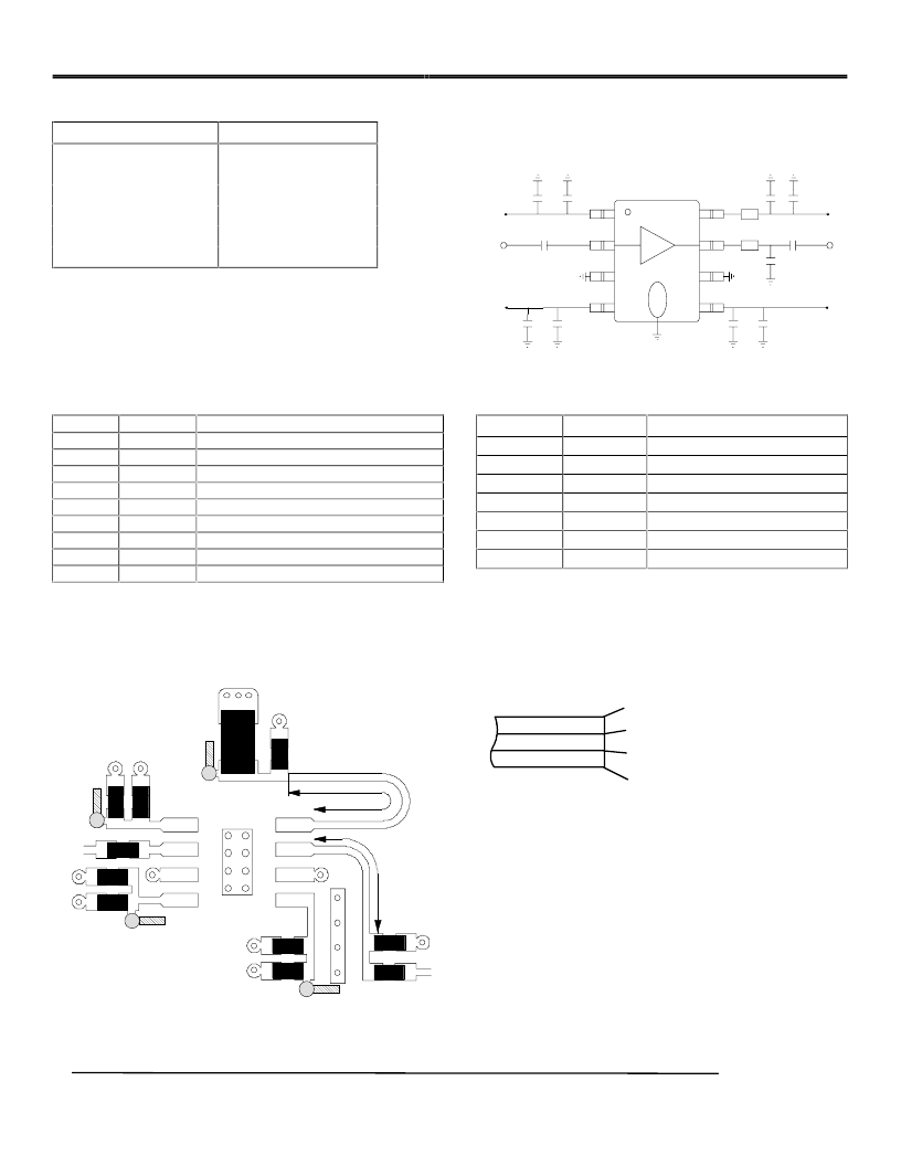
Pin Configuration
Pin No.
1
2
3
4
5
6
7
8
9
Pin Name
V
G1
RF IN
GND
V
D1
V
G2
GND
RF OUT
V
D2
Puck
Description
Negative supply voltage, First stage
RF Input of the amplifier
DC and RF Ground
Positive supply voltage, First stage
Negative supply voltage, First stage
DC and RF Ground
RF Output of the amplifier
Positive supply voltage, Second stage
DC and RF Ground
Recommended PCB Configuration
Layout View (AMPS 824-849 MHz)
0.47" (T1)
0.25" (T2)
C9
C8
C1
C6
C10
C3
C7
C11
C2
C4
C5
Functional Block Diagram
(AMPS 824-849 MHz)
1
2
4
3
8
7
5
6
C 1
C 2
C 3
C 4
C 5
C 6
C 7
C 8
C 9
C 1 1
R F O U T
R F IN
V D 1
V D 2
V G 2
V G 1
C 1 0
T 1
T 2
9
External Circuitry Parts List
(AMPS 824-849 MHz)
Part
C1 - C3
C4 - C7
C8
C9, C10
C11
T1
T2
1.) The recommended layout is specifically for the AMPS application. It
shows EIA code size 0603 standard SMT capacitors with the exception of
C11 which is a EIA code size 3528
2.) The location of C9, C10 and C11 is not critical to the performance of
the amplifier.
Value
220 pF
0.1 uF
8 pF
56 pF
1.0 uF
0.470”
0.250”
Purpose
By-Pass
By-Pass
Power Tuning
DC Block
By-Pass
Matching Transmission
Lines (50
)
Cross Section View
RF Traces + Components
RF Ground
DC Routing
Customer Defined
The PCB dielectric between RF traces and RF ground layers should
be chosen to reduce RF discontinuities between 50
lines and
package pins. M/A-COM recommends an FR-4 dielectric thickness
of 0.008”(0.2 mm) yielding a 50
line width of 0.015”(0.38 mm).
The recommended metalization thickness is 1 oz. copper and ground
metalization thickness is 2 oz.. Shaded traces are vias to DC
Routing layer and traces on DC Routing layer.
Biasing Procedure
The AM52-0001 requires that V
GG
bias be applied prior to
ANY
V
DD
bias. Permanent damage will occur if this procedure is not
followed. All FETs in the PA will draw IDSS and damage internal
circuitry. Resistance added in seiries with V
g1
and V
g2
may degrade
performance.
相關(guān)PDF資料 |
PDF描述 |
|---|---|
| AM52-0001SMB | 1.2 W High Efficiency Power Amplifier 800 - 960 MHz |
| AM52-0001TR | 1.2 W High Efficiency Power Amplifier 800 - 960 MHz |
| AM52-0002 | Industrial Control IC |
| AM52-0002TR | Industrial Control IC |
| AM52-0023SMB | Power Amplifier with T/R Switch for 802.11b |
相關(guān)代理商/技術(shù)參數(shù) |
參數(shù)描述 |
|---|---|
| AM52-0001SMB | 制造商:MA-COM 制造商全稱(chēng):M/A-COM Technology Solutions, Inc. 功能描述:1.2 W High Efficiency Power Amplifier 800 - 960 MHz |
| AM52-0001TR | 制造商:MA-COM 制造商全稱(chēng):M/A-COM Technology Solutions, Inc. 功能描述:1.2 W High Efficiency Power Amplifier 800 - 960 MHz |
| AM52-0002 | 制造商:未知廠家 制造商全稱(chēng):未知廠家 功能描述:Industrial Control IC |
| AM52-0002TR | 制造商:未知廠家 制造商全稱(chēng):未知廠家 功能描述:Industrial Control IC |
| AM52-0023 | 制造商:MA-COM 制造商全稱(chēng):M/A-COM Technology Solutions, Inc. 功能描述:Power Amplifier with T/R Switch for 802.11b |
發(fā)布緊急采購(gòu),3分鐘左右您將得到回復(fù)。