- 您現(xiàn)在的位置:買賣IC網(wǎng) > PDF目錄362278 > AM486DXPGA Am486DX PGA - Am486DX PGA Package Temperature Comparisons PDF資料下載
參數(shù)資料
| 型號: | AM486DXPGA |
| 英文描述: | Am486DX PGA - Am486DX PGA Package Temperature Comparisons |
| 中文描述: | Am486DX美巡賽- Am486DX PGA封裝溫度比較 |
| 文件頁數(shù): | 32/52頁 |
| 文件大?。?/td> | 1242K |
| 代理商: | AM486DXPGA |
第1頁第2頁第3頁第4頁第5頁第6頁第7頁第8頁第9頁第10頁第11頁第12頁第13頁第14頁第15頁第16頁第17頁第18頁第19頁第20頁第21頁第22頁第23頁第24頁第25頁第26頁第27頁第28頁第29頁第30頁第31頁當(dāng)前第32頁第33頁第34頁第35頁第36頁第37頁第38頁第39頁第40頁第41頁第42頁第43頁第44頁第45頁第46頁第47頁第48頁第49頁第50頁第51頁第52頁
32
Am486DE2 Microprocessor
I
To implement a 0-V suspend function, the system
must have access to all normal system memory from
within an SMI handler routine. If the SMRAM
overlays normal system memory (see Figure 14),
there must be a method to access overlaid system
memory independently.
The recommended configuration is to use a separate
(nonoverlaid) physical address for SMRAM. This non-
overlaid scheme prevents the CPU from improperly ac-
cessing the SMRAM or system RAM directly or through
the cache. Figure 15 shows the relative SMM timing for
nonoverlaid SMRAM for systems configured in Write-
through mode.
When the default SMRAM location is used, however,
SMRAM is overlaid with system main memory (at
38000h–3FFFFh). For simplicity, system designers may
want to use this default address, or they may select
another overlaid address range. However, in this case
the system control circuitry must use SMIACT to distin-
guish between SMRAM and main system memory, and
must restrict SMRAM space access to the CPU only. To
maintain cache coherency and to ensure proper system
operation in systems configured in Write-through mode,
the system must flush both the CPU internal cache and
any second-level caches in response to SMIACT going
Low. A system that uses cache during SMM must flush
the cache a second time in response to SMIACT going
High (see Figure 16). If KEN is driven High when FLUSH
is asserted, the cache is disabled and a second flush is
not required (see Figure 17).
Cache Flushes
The CPU does not unconditionally flush its cache before
entering SMM. Therefore, the designer must ensure
that, for systems using overlaid SMRAM, the cache is
flushed upon SMM entry, and SMM exit if caching is
enabled.
If the flush at SMM entry is not done, the first SMM read
could hit in a cache that contains normal memory space
code/data instead of the required SMI handler and the
handler could not be executed. If the cache is not dis-
abled and cache is not flushed at SMM exit, the normal
read cycles after SMM may hit in a cache that may con-
tain SMM code/data instead of the normal system mem-
ory contents.
In Write-through mode, assert the FLUSH signal in re-
sponse to the assertion of SMIACT at SMM entry, and
if required because the cache is enabled, assert FLUSH
again in response to the deassertion of SMIACT at SMM
exit (see Figure 16 and Figure 17).
Reloading the state registers at the end of SMM restores
cache functionality to its pre-SMM state.
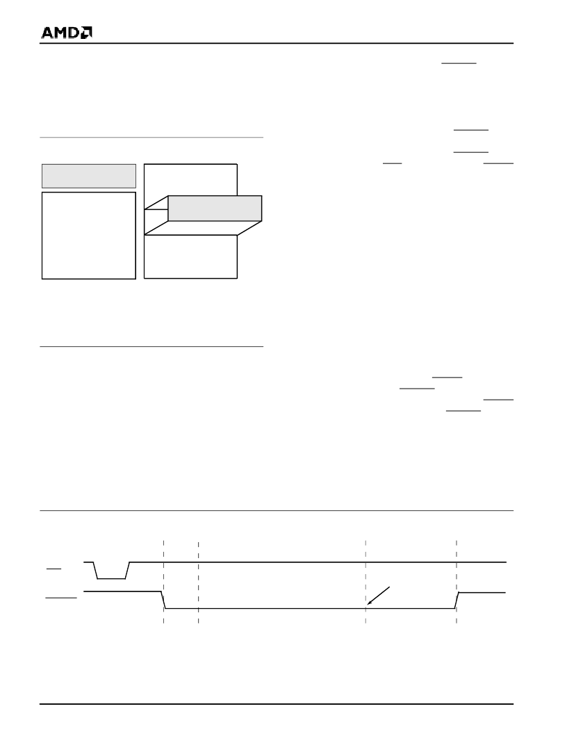
Figure 14. SMRAM Location
Non-overlaid
(no need to flush
caches)
Overlaid
(caches must
be flushed)
Normal
memory
Normal
memory
SMRAM
Normal
memory
Overlaid region
SMRAM
Figure 15. SMM Timing in Systems Using Non-Overlaid Memory Space and Write-Through Mode with
Caching Enabled During SMM
State
Save
SMI Handler
State Resume
Normal
Cycle
RSM
SMI
SMIACT
相關(guān)PDF資料 |
PDF描述 |
|---|---|
| AM486DXSQFP | 70NS, PLCC, IND TEMP(EEPROM) |
| AM486 | Am486 Microprocessor Software User's Manual? 4.40MB (PDF) |
| AM49DL3208G | Am49DL3208G - Stacked Multi-Chip Package (MCP) Flash Memory and pSRAM |
| AM49DL320BG | Am49DL320BG - Stacked Multi-Chip Package (MCP) Flash Memory and SRAM |
| AM49DL32XBG | Am49DL32xBG - Stacked Multi-Chip Package (MCP) Flash Memory and SRAM |
相關(guān)代理商/技術(shù)參數(shù) |
參數(shù)描述 |
|---|---|
| AM486DXSQFP | 制造商:未知廠家 制造商全稱:未知廠家 功能描述:Am486DX SQFP - Am486DX SQFP Package Temperature Comparisons |
| AM486-EVAL-KIT | 制造商:Advanced Micro Devices 功能描述:AM486CDP EVAL KIT |
| AM4874N | 制造商:ANALOGPOWER 制造商全稱:ANALOGPOWER 功能描述:N-Channel 30-V (D-S) MOSFET |
| AM4890N | 制造商:ANALOGPOWER 制造商全稱:ANALOGPOWER 功能描述:Dual N-Channel 150-V (D-S) MOSFET |
| AM4892N | 制造商:ANALOGPOWER 制造商全稱:ANALOGPOWER 功能描述:Dual N-Channel 150-V (D-S) MOSFET |
發(fā)布緊急采購,3分鐘左右您將得到回復(fù)。