- 您現(xiàn)在的位置:買賣IC網(wǎng) > PDF目錄362246 > AM29F100AT-70SC 30V Single N-Channel HEXFET Power MOSFET in a SOT-223 package; A IRLL3303 with Standard Packaging PDF資料下載
參數(shù)資料
| 型號: | AM29F100AT-70SC |
| 英文描述: | 30V Single N-Channel HEXFET Power MOSFET in a SOT-223 package; A IRLL3303 with Standard Packaging |
| 中文描述: | x8/x16閃存EEPROM |
| 文件頁數(shù): | 33/39頁 |
| 文件大小: | 728K |
| 代理商: | AM29F100AT-70SC |
第1頁第2頁第3頁第4頁第5頁第6頁第7頁第8頁第9頁第10頁第11頁第12頁第13頁第14頁第15頁第16頁第17頁第18頁第19頁第20頁第21頁第22頁第23頁第24頁第25頁第26頁第27頁第28頁第29頁第30頁第31頁第32頁當(dāng)前第33頁第34頁第35頁第36頁第37頁第38頁第39頁
Am29F002B/Am29F002NB
33
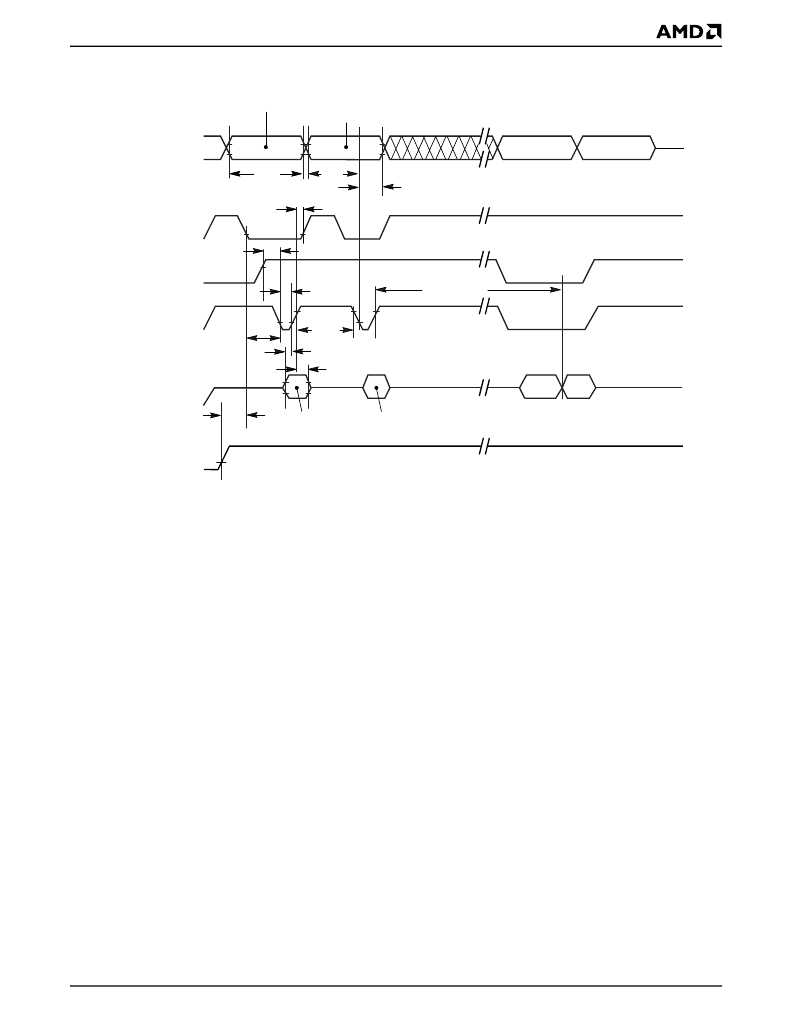
AC CHARACTERISTICS
t
GHEL
t
WS
OE#
CE#
WE#
RESET#
t
DS
Data
t
AH
Addresses
t
DH
t
CP
DQ7#
D
OUT
t
WC
t
AS
t
CPH
PA
Data# Polling
A0 for program
55 for erase
t
RH
t
WHWH1 or 2
t
WH
PD for program
30 for sector erase
10 for chip erase
555 for program
2AA for erase
PA for program
SA for sector erase
555 for chip erase
Notes:
1. PA = Program Address, PD = Program Data, DQ7# = complement of data written to device, D
OUT
= data written to device.
2. Figure indicates the last two bus cycles of the command sequence.
Figure 17.
Alternate CE# Controlled Write Operation Timings
相關(guān)PDF資料 |
PDF描述 |
|---|---|
| AM29F100AT-70SE | 30V Single N-Channel HEXFET Power MOSFET in a SOT-223 package; Similar to IRLL3303 with Lead Free Packaging |
| AM29F100AT-70SI | x8/x16 Flash EEPROM |
| AM29F100AT-90EC | 20V Single N-Channel HEXFET Power MOSFET in a TO-220AB package; A IRL3102 with Standard Packaging |
| AM29F100AT-90EE | x8/x16 Flash EEPROM |
| AM29F100AT-90EI | 100V Single N-Channel HEXFET Power MOSFET in a TO-220AB package; A IRL530N with Standard Packaging |
相關(guān)代理商/技術(shù)參數(shù) |
參數(shù)描述 |
|---|---|
| AM29F100B120EC | 制造商:AMD 功能描述:* |
| AM29F100B-120EC | 制造商:Advanced Micro Devices 功能描述: |
| AM29F100B120SC | 制造商:AMD 功能描述:New |
| AM29F100B-120SC | 制造商:Advanced Micro Devices 功能描述:NOR Flash, 64K x 16, 44 Pin, Plastic, SOP |
| AM29F100B90SIT | 制造商:AMD 功能描述:New |
發(fā)布緊急采購,3分鐘左右您將得到回復(fù)。