- 您現(xiàn)在的位置:買賣IC網(wǎng) > PDF目錄374022 > ADP3522 (Analog Devices, Inc.) GSM Power Management System PDF資料下載
參數(shù)資料
| 型號: | ADP3522 |
| 廠商: | Analog Devices, Inc. |
| 元件分類: | 基準(zhǔn)電壓源/電流源 |
| 英文描述: | GSM Power Management System |
| 中文描述: | 手機電源管理系統(tǒng) |
| 文件頁數(shù): | 6/20頁 |
| 文件大小: | 467K |
| 代理商: | ADP3522 |
REV. 0
–6–
ADP3522
CAUTION
ESD (electrostatic discharge) sensitive device. Electrostatic charges as high as 4000 V readily
accumulate on the human body and test equipment and can discharge without detection. Although the
ADP3522 features proprietary ESD protection circuitry, permanent damage may occur on devices
subjected to high energy electrostatic discharges. Therefore, proper ESD precautions are recommended
to avoid performance degradation or loss of functionality.
ABSOLUTE MAXIMUM RATINGS
*
Voltage on Any Pin with Respect to
Any GND Pin . . . . . . . . . . . . . . . . . . . . . . . –0.3 V to +10 V
Voltage on Any Pin May Not Exceed VBAT, with the Following
Exceptions: CHRIN, BASE, ISENSE
Storage Temperature Range . . . . . . . . . . . . .–65
∞
C to +150
∞
C
Operating Ambient Temperature Range . . . . .–20
∞
C to +85
∞
C
Maximum Junction Temperature . . . . . . . . . . . . . . . . . 125
∞
C
JA
, Thermal Impedance (LFCSP 5 mm 5 mm)
4-Layer JEDEC PCB . . . . . . . . . . . . . . . . . . . . . . . . . . 32
∞
C/W
2-Layer SEMI PCB . . . . . . . . . . . . . . . . . . . . . . . . . . 108
∞
C/W
Lead Temperature Range (Soldering, 60 sec.) . . . . . . . . 300
∞
C
*
Stresses above those listed under Absolute Maximum Ratings may cause perma-
nent damage to the device. This is a stress rating only; functional operation of the
device at these or any other conditions above those listed in the operational
sections of this specification is not implied. Exposure to absolute maximum rating
conditions for extended periods may affect device reliability. Absolute maximum
ratings apply individually only, not in combination. Unless otherwise specified all
other voltages are referenced to GND.
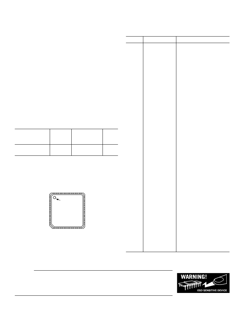
PIN CONFIGURATION
TOP VIEW
1
2
3
4
5
6
7
8
ADP3522
24
23
22
21
20
19
18
17
9
1
G
1
D
1
I
1
E
1
C
1
R
1
R
3
3
3
2
2
2
2
2
PIN 1
INDICATOR
SIMEN
VRTCIN
VRTC
BATSNS
MVBAT
CHRDET
CHRIN
SIMVSEL
NC
VAN
VBAT
VCORE
VMEM
VBAT2
VSIM
NC
G
N
R
P
P
T
A
R
V
ORDERING GUIDE
Memory
LDO
Output
Temperature
Range
–20
∞
C to +85
∞
C
–20
∞
C to +85
∞
C
Package
Option
Model
ADP3522ACP-3
ADP3522ACP-1.8
2.80 V
1.80 V
CP-32
CP-32
PIN FUNCTION DESCRIPTIONS
Pin
Mnemonic
Description
1
2
3
SIMEN
VRTCIN
VRTC
SIM LDO Enable
RTC LDO Input Voltage
Real-Time Clock Supply/
Coin Cell Battery Charger
Battery Voltage Sense Input
Divided Battery Voltage Output
Charge Detect Output
Charger Input Voltage
Programs VSIM Output;
Low: 1.8 V
Charger Drive Output
Microprocessor Charger Gate
Control Input
Digital Ground
Charge Current Sense Input
End of Charge Output
Charge Enable Control Input
Reset Delay Time
Main Reset, Open Drain
No Connection
SIM LDO Output
Battery Input Voltage 2
Memory LDO Output
Digital Core LDO Output
Battery Input Voltage
Analog LDO Output
TCXO LDO Output
Output Reference
Analog Ground
TCXO LDO Enable and
MVBAT Enable
Power On/Off Signal from
Microprocessor
Power On/Off Key
Power Key Interface Output
4
5
6
7
8
BATSNS
MVBAT
CHRDET
CHRIN
SIMVSEL
9
10
GATEDR
GATEIN
11
12
13
14
15
16
17, 24, 32
18
19
20
21
22
23
25
26
27
28
DGND
ISENSE
EOC
CHGEN
RESCAP
RESET
NC
VSIM
VBAT2
VMEM
VCORE
VBAT
VAN
VTCXO
REFOUT
AGND
TCXOEN
29
PWRONIN
30
31
PWRONKEY
ROWX
相關(guān)PDF資料 |
PDF描述 |
|---|---|
| ADP3522ACP-1.8 | GSM Power Management System |
| ADP3522ACP-3 | GSM Power Management System |
| ADP3604 | |
| ADP3604AR | Secondary Over-Voltage Protection for 2-4 cell in series Li-Ion/Poly (4.45V) 8-SM8 -40 to 110 |
| ADP3604* | Dual/Quad Rail-to-Rail Output, Picoamp Input Precision Op Amps; Package: SO; No of Pins: 8; Temperature Range: -40°C to +85°C |
相關(guān)代理商/技術(shù)參數(shù) |
參數(shù)描述 |
|---|---|
| ADP3522ACP-1.8 | 制造商:AD 制造商全稱:Analog Devices 功能描述:GSM Power Management System |
| ADP3522ACP-1.8-RL | 制造商:Analog Devices 功能描述:GSM Power Management System 32-Pin LFCSP EP T/R |
| ADP3522ACP-1.8-RL7 | 制造商:Analog Devices 功能描述:GSM Power Management System 32-Pin LFCSP EP T/R |
| ADP3522ACP-3 | 制造商:AD 制造商全稱:Analog Devices 功能描述:GSM Power Management System |
| ADP3522ACP-3-REEL | 制造商:Analog Devices 功能描述:GSM Power Management System 32-Pin LFCSP EP T/R |
發(fā)布緊急采購,3分鐘左右您將得到回復(fù)。