- 您現(xiàn)在的位置:買賣IC網(wǎng) > PDF目錄374022 > ADP3419JRM-REEL (ANALOG DEVICES INC) Dual Bootstrapped, High Voltage MOSFET Driver with Output Disable PDF資料下載
參數(shù)資料
| 型號: | ADP3419JRM-REEL |
| 廠商: | ANALOG DEVICES INC |
| 元件分類: | MOSFETs |
| 英文描述: | Dual Bootstrapped, High Voltage MOSFET Driver with Output Disable |
| 中文描述: | HALF BRDG BASED MOSFET DRIVER, PDSO10 |
| 封裝: | MSOP-10 |
| 文件頁數(shù): | 3/16頁 |
| 文件大小: | 317K |
| 代理商: | ADP3419JRM-REEL |
ADP3419
SPECIFICATIONS
VCC = SD = 5 V, BST = 4 V to 26 V, T
A
= 0°C to 100°C, unless otherwise noted.
Rev. A | Page 3 of 16
All limits at temperature extremes are guaranteed via correlation using standard statistical quality control (SQC) methods.
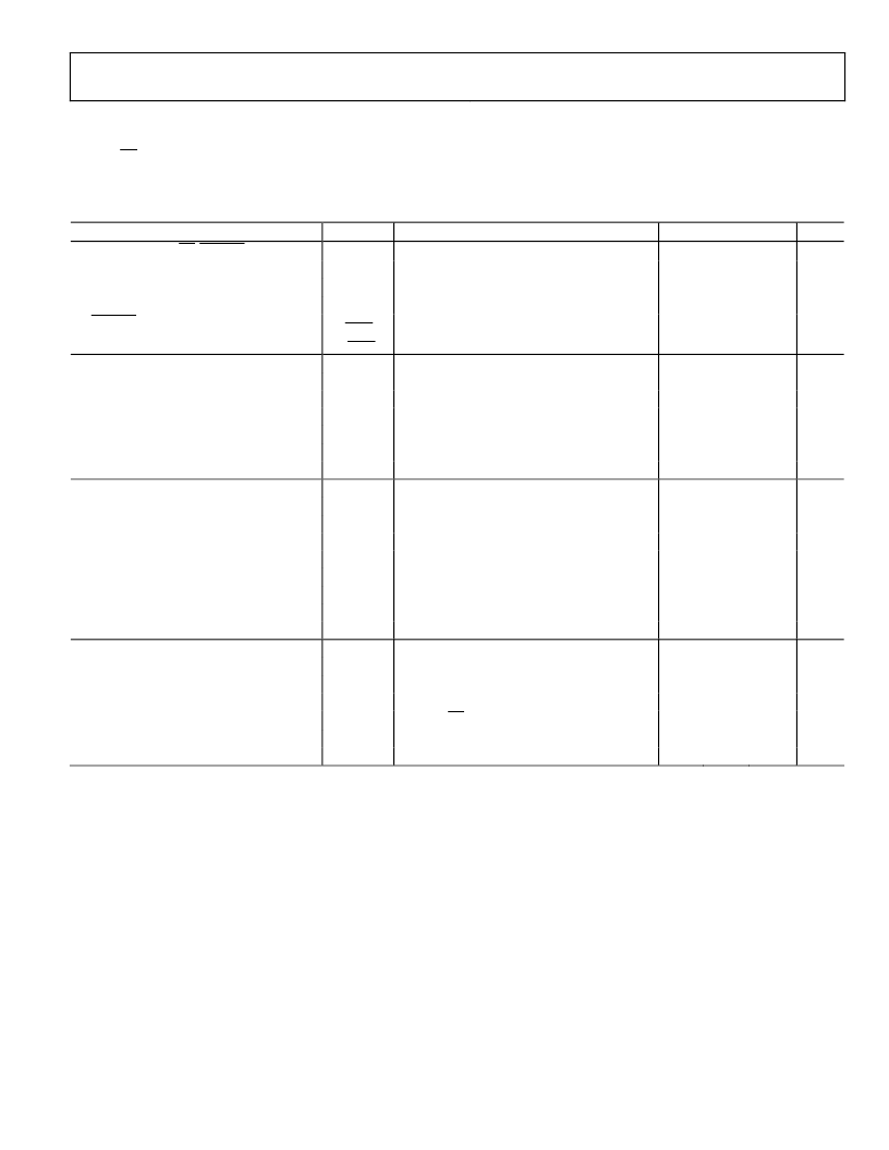
Table 1.
Parameter
Symbol
Conditions
LOGIC INPUTS (IN, SD, DRVLSD, CROWBAR)
Input Voltage High
V
IH
Input Voltage Low
V
IL
Input Current
I
IN
Inputs = 0 V or 5 V
DRVLSD Propagation Delay Time
t
pdlDRVLSD
,
t
pdhDRVLSD
HIGH-SIDE DRIVER
Output Resistance, Sourcing Current
BST SW = 4.6 V
Output Resistance, Sinking Current
BST SW = 4.6 V
Transition Times
t
rDRVH
BST SW = 4.6 V, C
LOAD
= 3 nF, Figure 4
t
fDRVH
BST SW = 4.6 V, C
LOAD
= 3 nF, Figure 4
Propagation Delay Times
1
t
pdhDRVH
BST SW = 4.6 V, C
LOAD
= 3 nF, Figure 4
t
pdlDRVH
BST SW = 4.6 V, C
LOAD
= 3 nF, Figure 4
LOW-SIDE DRIVER
Output Resistance, Sourcing Current
Output Resistance, Sinking Current
Transition Times
t
rDRVL
C
LOAD
= 3 nF, Figure 4
t
fDRVL
C
LOAD
= 3 nF, Figure 4
Propagation Delay Times
1, 2
t
pdhDRVL
C
LOAD
= 3 nF, Figure 4
t
pdlDRVL
C
LOAD
= 3 nF, Figure 4
SW Transition Timeout
2
t
SWTO
BST SW = 4.6 V
Zero-Crossing Threshold
V
ZC
SUPPLY
Supply Voltage Range
V
CC
Supply Current
Normal Mode
I
SYS(NM)
I
CC
+ I
BST
, IN = 0 V or 5 V
Shutdown Mode
I
SYS(SD)
I
CC
+ I
BST
, SD = 0 V
Undervoltage Lockout Threshold
VCC rising
Undervoltage Lockout Hysteresis
3
VCC falling
Min
2.0
1
Typ
20
Max
0.8
+1
Unit
V
V
μA
ns
C
LOAD
= 3 nF, Figure 3
15
150
4.6
3.8
50
1.7
0.8
14
11
32
28
1.7
0.8
13
11
25
16
350
1
0.8
325
4.25
120
3.3
2.3
35
25
70
60
3.3
2.3
30
25
48
30
600
6
1.5
600
4.5
ns
ns
ns
ns
ns
ns
ns
ns
ns
V
V
mA
μA
V
mV
1
For propagation delays, t
pdh
refers to the specified signal going high, and t
pdl
refers to the signal going low with transitions measured at 50%.
2
The turn-on of DRVL is initiated after IN goes low by either SW crossing a ~1 V threshold or by expiration of t
SWTO
.
3
Guaranteed by characterization, not production tested.
相關(guān)PDF資料 |
PDF描述 |
|---|---|
| ADP3419JRMZ-REEL1 | Dual Bootstrapped, High Voltage MOSFET Driver with Output Disable |
| ADP3421 | Geyserville-Enabled DC-DC Converter Controller for Mobile CPUs |
| ADP3421JRU | Geyserville-Enabled DC-DC Converter Controller for Mobile CPUs |
| ADP3422 | Secondary Over-Voltage Protection for 2-4 cell in series Li-Ion/Poly (4.35V) 8-TSSOP -40 to 110 |
| ADP3422JRU | Secondary Over-Voltage Protection for 2-4 cell in series Li-Ion/Poly (4.40V) 8-SM8 -40 to 110 |
相關(guān)代理商/技術(shù)參數(shù) |
參數(shù)描述 |
|---|---|
| ADP3419JRMZ | 制造商:Analog Device 功能描述: 制造商:Analog Devices 功能描述:MOSFET Driver, Dual, 10 Pin, Plastic, TSSOP |
| ADP3419JRMZ-REEL | 功能描述:功率驅(qū)動器IC DUAL SYNCHRONOUS DRV RoHS:否 制造商:Micrel 產(chǎn)品:MOSFET Gate Drivers 類型:Low Cost High or Low Side MOSFET Driver 上升時間: 下降時間: 電源電壓-最大:30 V 電源電壓-最小:2.75 V 電源電流: 最大功率耗散: 最大工作溫度:+ 85 C 安裝風(fēng)格:SMD/SMT 封裝 / 箱體:SOIC-8 封裝:Tube |
| ADP3419JRMZ-REEL1 | 制造商:AD 制造商全稱:Analog Devices 功能描述:Dual Bootstrapped, High Voltage MOSFET Driver with Output Disable |
| ADP34200002RUR | 制造商:Rochester Electronics LLC 功能描述:- Bulk |
| ADP3421 | 制造商:AD 制造商全稱:Analog Devices 功能描述:Geyserville-Enabled DC-DC Converter Controller for Mobile CPUs |
發(fā)布緊急采購,3分鐘左右您將得到回復(fù)。