- 您現(xiàn)在的位置:買賣IC網(wǎng) > PDF目錄373995 > ADM1060ARU (ANALOG DEVICES INC) CON-HDR64POS2ROW 4WALL.1X.1SP,RTANG,LOPF PDF資料下載
參數(shù)資料
| 型號: | ADM1060ARU |
| 廠商: | ANALOG DEVICES INC |
| 元件分類: | 電源管理 |
| 英文描述: | CON-HDR64POS2ROW 4WALL.1X.1SP,RTANG,LOPF |
| 中文描述: | 7-CHANNEL POWER SUPPLY MANAGEMENT CKT, PDSO28 |
| 封裝: | MO-153AE, TSSOP-28 |
| 文件頁數(shù): | 41/45頁 |
| 文件大小: | 303K |
| 代理商: | ADM1060ARU |
第1頁第2頁第3頁第4頁第5頁第6頁第7頁第8頁第9頁第10頁第11頁第12頁第13頁第14頁第15頁第16頁第17頁第18頁第19頁第20頁第21頁第22頁第23頁第24頁第25頁第26頁第27頁第28頁第29頁第30頁第31頁第32頁第33頁第34頁第35頁第36頁第37頁第38頁第39頁第40頁當(dāng)前第41頁第42頁第43頁第44頁第45頁
PROGRAMMNGADM1060
ADM1060
–
41
–
REV. PrJ 11/02
PRELIMINARY TECHNICAL DATA
this case the command byte is the high byte of the
EEPROM address from F8h to F9h. T he (only) data
byte is the low byte of the EEPROM address. T his is
illustrated in Figure 9c.
S
SLAVE
ADDRESS
W A
EEPROM
ADDRESS
HIGH BYTE
(F8h TO F9h)
EEPROM
ADDRESS
LOW BYTE
(00h TO FFh)
A
A P
1
2
3
4
5
6
7
8
Figure 9d. Setting An EEPROM Address
Note for page erasure that as a page consists of 32
bytes only the three MSB
’
s of the address low byte are
important. T he lower 5 bits of the EEPROM address
low byte only specify addresses within a page and are
ignored during an erase operation.
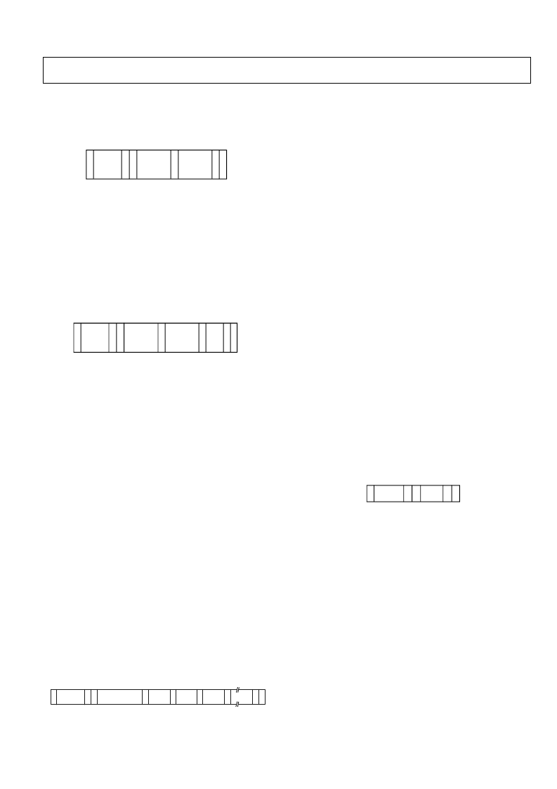
3. Write a single byte of data to EEPROM. In this case
the command byte is the high byte of the EEPROM
address from F8h to F9h. T he first data byte is the low
byte of the EEPROM address and the second data byte
is the actual data. T his is illustrated in Figure 9e.
S
SLAVE
ADDRESS
W A
EEPROM
ADDRESS
HIGH BYTE
(F8h TO F9h)
EEPROM
ADDRESS
LOW BYTE
(00h TO FFh)
A
A DATA A P
1
2
3
4
5
6
7
8
9 10
Figure 9e. Single Byte Write To EEPROM
Block Write
In this operation the master device writes a block of data
to a slave device. T he start address for a block write must
previously have been set. In the case of the ADM1060 this
is done by a Send Byte operation to set a RAM address or
a Write Byte/Word operation to set an EEPROM address.
1. T he master device asserts a start condition on SDA.
2. T he master sends the 7-bit slave address followed by
the write bit (low).
3. T he addressed slave device asserts ACK on SDA.
4. T he master sends a command code that tells the slave
device to expect a block write. T he ADM1060 com-
mand code for a block write is FCh (11111100).
5. T he slave asserts ACK on SDA.
6. T he master sends a data byte that tells the slave device
how many data bytes will be sent. T he SMBus specifi-
cation allows a maximum of 32 data bytes to be sent in
a block write.
7. T he slave asserts ACK on SDA.
8. T he master sends N data bytes.
9. The slave asserts ACK on SDA after each data byte.
10. The master asserts a STOP condition on SDA to end the
transaction.
S
SLAVE
ADDRESSW A(BLOCK WRITE)
BYTE
COUNT
A
A
DATA 1
A
P
A
DATA 2
DATA N A
1
2
3
4
5
6
7
8
9
10
Figure 9f. Block Write To EEPROM Or RAM
Unlike some EEPROM devices which limit block writes to
within a page boundary, there is no limitation on the start
address when performing a block write to EEPROM, except:
1. T here must be at least N locations from the start ad-
dress to the highest EEPROM address (F9FFh), to avoid-
ing writing to invalid addresses.
2. If the addresses cross a page boundary, both pages must
be erased before programming.
Note that the ADM1060 features a clock extend function
for writes to EEPROM. Programming an EEPROM byte
takes approximately 250μs, which would limit the SMBus
clock for repeated or block write operations. T he
ADM1060 pulls SCL low and extends the clock pulse
when it cannot accept any more data.
A D M1060 R E A D OPE R A T IONS
T he ADM1060 uses the following SMBus read protocols:
R E C E IVE BY T E
In this operation the master device receives a single byte
from a slave device, as follows:
1.T he master device asserts a ST ART condition on SDA.
2.T he master sends the 7-bit slave address followed by the
read bit (high).
3.T he addressed slave device asserts ACK on SDA.
4.T he master receives a data byte.
5.T he master asserts NO ACK on SDA.
6.T he master asserts a ST OP condition on SDA and the
transaction ends.
In the ADM1060, the receive byte protocol is used to read
a single byte of data from a RAM or EEPROM location
whose address has previously been set by a send byte or
write byte/word operation. T his is illustrated in Figure 9g.
S
SLAVE
ADDRESS
R
A
DATA
A
P
1
2
3
4
5
6
Figure 9g. Single Byte Read From EEPROM Or RAM
Block Read
In this operation the master device reads a block of data
from a slave device. T he start address for a block read
must previously have been set. In the case of the
ADM1060 this is done by a Send Byte operation to set a
RAM address, or a Write Byte/Word operation to set an
EEPROM address. T he block read operation itself
consists of a Send Byte operation that sends a block read
command to the slave, immediately followed by a repeated
start and a read operation that reads out multiple data
bytes, as follows:
1.T he master device asserts a ST ART condition on SDA.
2.T he master sends the 7-bit slave address followed by the
write bit (low).
3.T he addressed slave device asserts ACK on SDA.
4.T he master sends a command code that tells the slave
device to expect a block read. T he ADM1060 command
code for a block read is FDh (11111101).
相關(guān)PDF資料 |
PDF描述 |
|---|---|
| ADM1064 | Super Sequencer with Voltage Readback ADC |
| ADM1064ACP | Super Sequencer with Voltage Readback ADC |
| ADM1064ACP-REEL | Super Sequencer with Voltage Readback ADC |
| ADM1064ACP-REEL7 | Super Sequencer with Voltage Readback ADC |
| ADM1064ASU | Super Sequencer with Voltage Readback ADC |
相關(guān)代理商/技術(shù)參數(shù) |
參數(shù)描述 |
|---|---|
| ADM1060ARUCS0001R7 | 功能描述:IC SUPERVISOR/SEQUENCER 制造商:analog devices inc. 系列:* 零件狀態(tài):上次購買時間 標(biāo)準(zhǔn)包裝:1 |
| ADM1060ARUCS0100R7 | 功能描述:IC SUPERVISOR/SEQUENCER 制造商:analog devices inc. 系列:* 零件狀態(tài):上次購買時間 標(biāo)準(zhǔn)包裝:1 |
| ADM1060ARUCS0101R7 | 功能描述:IC SUPERVISOR/SEQUENCER 制造商:analog devices inc. 系列:* 零件狀態(tài):上次購買時間 標(biāo)準(zhǔn)包裝:1 |
| ADM1060ARUCS0102R7 | 功能描述:IC SUPERVISOR/SEQUENCER 制造商:analog devices inc. 系列:* 零件狀態(tài):上次購買時間 標(biāo)準(zhǔn)包裝:1 |
| ADM1060ARUCS0103R7 | 制造商:Analog Devices 功能描述: |
發(fā)布緊急采購,3分鐘左右您將得到回復(fù)。