- 您現(xiàn)在的位置:買賣IC網(wǎng) > PDF目錄378285 > ADC14071CIVBH (NATIONAL SEMICONDUCTOR CORP) 14-Bit, 7 MSPS, 380 mW A/D Converter PDF資料下載
參數(shù)資料
| 型號: | ADC14071CIVBH |
| 廠商: | NATIONAL SEMICONDUCTOR CORP |
| 元件分類: | ADC |
| 英文描述: | 14-Bit, 7 MSPS, 380 mW A/D Converter |
| 中文描述: | 1-CH 14-BIT PROPRIETARY METHOD ADC, PARALLEL ACCESS, PQFP48 |
| 封裝: | TQFP-48 |
| 文件頁數(shù): | 17/18頁 |
| 文件大小: | 427K |
| 代理商: | ADC14071CIVBH |
Applications Information
(Continued)
7.0 COMMON APPLICATION PITFALLS
Driving the inputs (analog or digital) beyond the power
supply rails.
For proper operation, all inputs should not go
more than 300 mV beyond the supply rails (more than 300
mV below the ground pins or 300 mV above the supply pins).
Exceeding these limits on even a transient basis may cause
faulty or erratic operation. It is not uncommon for high speed
digital circuits (e.g., 74F and 74AC devices) to exhibit over-
shoot or undershoot that goes above the power supply or
more than a volt below ground. A resistor of about 50
to
100
in series with the offending digital input will eliminate
the problem.
Do not allow input voltages to exceed the supply voltage,
even on a transient basis. Not even during power up.
Be careful not to overdrive the inputs of the ADC14071 with
a device that is powered from supplies outside the range of
the ADC14071 supply. Such practice may lead to conversion
inaccuracies and even to device damage.
Attempting to drive a high capacitance digital data bus.
The more capacitance the output drivers must charge for
each conversion, the more instantaneous digital current
flows through DR V
and DR GND. These large charging
current spikes can couple into the analog circuitry, degrading
dynamic performance. Adequate bypassing and maintaining
separate analog and digital ground planes will reduce this
problem.
Additionally, bus capacitance beyond the specified 20 pF/pin
will cause t
to increase, making it difficult to properly latch
theADC output data. The result could, again, be an apparent
reduction in dynamic performance.
The digital data outputs should be buffered (with 74ACQ541,
for example). Dynamic performance can also be improved
by adding series resistors at each digital output, close to the
ADC14071, which reduces the energy coupled back into the
converter output pins by limiting the output current.Areason-
able value for these resistors is 47
.
Using an inadequate amplifier to drive the analog input.
As explained in Section 1.3, the capacitance seen at the in-
put alternates between 14 pF and 5 pF, depending upon the
phase of the clock. This dynamic load is more difficult to
drive than is a fixed capacitance.
If the amplifier exhibits overshoot, ringing, or any evidence of
instability, even at a very low level, it will degrade perfor-
mance. A small series resistor at each amplifier output and a
capacitor across the analog inputs (as shown in Figures 6, 7)
will improve performance. The LM6172 has been success-
fully used to drive the analog inputs of the ADC14071.
Also, it is important that te signals at the two inputs have ex-
actly the same amplitude and be exactly 180 out of phase
with each other. Board layout, especially equality of the
length of the two traces to the input pins, will affect the effec-
tive phase between these two signals. Remember that an
operational amplifier operated in the non-inverting configura-
tion will exhibit more time delay than will the same device op-
erating in the inverting configuration.
Operating with the reference pins outside of the speci-
fied range.
As mentioned in Section 1.2, V
REF
should be in
the range of
1.0V
≤
V
REF
≤
2.7V.
Operating outside of these limits could lead to performance
degradation.
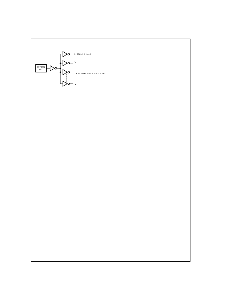
Using a clock source with excessive jitter, using exces-
sively long clock signal trace, or having other signals
coupled to the clock signal trace.
This will cause the sam-
pling interval to vary, causing excessive output noise and a
reduction in SNR performance.
DS101101-29
FIGURE 9. Isolating the ADC Clock from other Circuitry
with A Clock Tree
A
www.national.com
17
相關(guān)PDF資料 |
PDF描述 |
|---|---|
| ADC14071 | 14-Bit, 7 MSPS, 380 mW A/D Converter |
| ADC14071EVAL | 14-Bit, 7 MSPS, 380 mW A/D Converter |
| ADC14161 | Low Dropout Linear 2-cell Li-Ion Charge Controller with AutoCompTM, 8.4V 8-SOIC -20 to 70 |
| ADC14161CIVT | Low-Distortion, Self-Calibrating 14-Bit, 2.5 MSPS, 390 mW A/D Converter |
| ADC16061CCVT | Self-Calibrating 16-Bit, 2.5 MSPS, 390 mW A/D Converter |
相關(guān)代理商/技術(shù)參數(shù) |
參數(shù)描述 |
|---|---|
| ADC1410S065/DB,598 | 功能描述:數(shù)據(jù)轉(zhuǎn)換 IC 開發(fā)工具 ADC DEMO BOARD RoHS:否 制造商:Texas Instruments 產(chǎn)品:Demonstration Kits 類型:ADC 工具用于評估:ADS130E08 接口類型:SPI 工作電源電壓:- 6 V to + 6 V |
| ADC1410S065F1-DB | 功能描述:ADC1410S065 - 14 Bit 65M Samples per Second Analog to Digital Converter (ADC) Evaluation Board 制造商:idt, integrated device technology inc 系列:- 零件狀態(tài):過期 A/D 轉(zhuǎn)換器數(shù):1 位數(shù):14 采樣率(每秒):65M 數(shù)據(jù)接口:SPI 輸入范圍:2 Vpp 不同條件下的功率(典型值):380mW @ 65MSPS 使用的 IC/零件:ADC1410S065 所含物品:板 標(biāo)準(zhǔn)包裝:1 |
| ADC1410S065F2-DB | 功能描述:ADC1410S065 - 14 Bit 65M Samples per Second Analog to Digital Converter (ADC) Evaluation Board 制造商:idt, integrated device technology inc 系列:- 零件狀態(tài):過期 A/D 轉(zhuǎn)換器數(shù):1 位數(shù):14 采樣率(每秒):65M 數(shù)據(jù)接口:SPI 輸入范圍:2 Vpp 不同條件下的功率(典型值):380mW @ 65MSPS 使用的 IC/零件:ADC1410S065 所含物品:板 標(biāo)準(zhǔn)包裝:1 |
| ADC1410S065HN,518 | 功能描述:模數(shù)轉(zhuǎn)換器 - ADC SNGLE 14b ADC 65MSPS RoHS:否 制造商:Texas Instruments 通道數(shù)量:2 結(jié)構(gòu):Sigma-Delta 轉(zhuǎn)換速率:125 SPs to 8 KSPs 分辨率:24 bit 輸入類型:Differential 信噪比:107 dB 接口類型:SPI 工作電源電壓:1.7 V to 3.6 V, 2.7 V to 5.25 V 最大工作溫度:+ 85 C 安裝風(fēng)格:SMD/SMT 封裝 / 箱體:VQFN-32 |
| ADC1410S065HN/C1,5 | 功能描述:模數(shù)轉(zhuǎn)換器 - ADC SGL 14b ADC 65 MSPS CMOS OR LVDS DDR RoHS:否 制造商:Texas Instruments 通道數(shù)量:2 結(jié)構(gòu):Sigma-Delta 轉(zhuǎn)換速率:125 SPs to 8 KSPs 分辨率:24 bit 輸入類型:Differential 信噪比:107 dB 接口類型:SPI 工作電源電壓:1.7 V to 3.6 V, 2.7 V to 5.25 V 最大工作溫度:+ 85 C 安裝風(fēng)格:SMD/SMT 封裝 / 箱體:VQFN-32 |
發(fā)布緊急采購,3分鐘左右您將得到回復(fù)。