- 您現(xiàn)在的位置:買賣IC網(wǎng) > PDF目錄378284 > ADC12L034CIWM (NATIONAL SEMICONDUCTOR CORP) 3.3V Self-Calibrating 12-Bit Plus Sign Serial I/O A/D Converters with MUX and Sample/Hold PDF資料下載
參數(shù)資料
| 型號: | ADC12L034CIWM |
| 廠商: | NATIONAL SEMICONDUCTOR CORP |
| 元件分類: | ADC |
| 英文描述: | 3.3V Self-Calibrating 12-Bit Plus Sign Serial I/O A/D Converters with MUX and Sample/Hold |
| 中文描述: | 4-CH 12-BIT SUCCESSIVE APPROXIMATION ADC, SERIAL ACCESS, PDSO24 |
| 封裝: | SOP-24 |
| 文件頁數(shù): | 26/36頁 |
| 文件大?。?/td> | 828K |
| 代理商: | ADC12L034CIWM |
第1頁第2頁第3頁第4頁第5頁第6頁第7頁第8頁第9頁第10頁第11頁第12頁第13頁第14頁第15頁第16頁第17頁第18頁第19頁第20頁第21頁第22頁第23頁第24頁第25頁當(dāng)前第26頁第27頁第28頁第29頁第30頁第31頁第32頁第33頁第34頁第35頁第36頁
Application Hints
(Continued)
in the power-down state. If a software power down instruc-
tion is issued to the ADC while a hardware power up is in ef-
fect (PD pin low), the device will power down. When the de-
vice is powered down by software, it may be powered up by
either issuing a software power up instruction or by taking
PD pin high and then low. If the power down command is is-
sued during an A/D conversion, that conversion is disrupted.
Therefore, the data output after power up cannot be relied
on.
1.6 User Mode and Test Mode
An instruction may be issued to the ADC to put it into test
mode. Test mode is used by the manufacturer to verify com-
plete functionality of the device. During test mode CH0–CH7
become active outputs. If the device is inadvertently put into
the test mode with CS low continuously, the serial communi-
cations may be desynchronized. Synchronization may be re-
gained by cycling the power supply voltage to the device.
Cycling the power supply voltage will also set the device into
user mode. If CS is used in the serial interface, theADC may
be queried to see what mode it is in. This is done by issuing
a “read STATUS register” instruction to the ADC. When bit 9
of the status register is high the ADC is in test mode; when
bit 9 is low the ADC is in user mode. As an alternative to cy-
cling the power supply, an instruction sequence may be used
to return the device to user mode. This instruction sequence
must be issued to the ADC using CS.
The following table lists the instructions required to return the
device to user mode:
Instruction
DI Data
DI3
X
L
L
L
L
L
DI0
H
L
L
L
L
L
H
or
L
H
or
L
H
or
L
DI1
X
L
L
L
L
L
DI2
X
L
L
L
L
L
DI4
H
H
H
H
H
H
DI5
H
H
L
L
H
L
DI6
H
H
H
H
H
H
DI7
H
L
L
H
H
L
TEST MODE
RESET
TEST MODE
INSTRUCTIONS
USER MODE
Power Up
Set DO with
or without
Sign
Set
Acquisition
Time
Start
a
Conversion
L
L
L
H
H
L
H
H
or
L
H
or
L
L
L
H
H
H
L
H
or
L
H
or
L
H
or
L
H
or
L
H
or
L
L
X = Don’t Care
After returning to user mode with the user mode instruction
the power up, data with or without sign, and acquisition time
instructions need to be resent to ensure that the ADC is in
the required state before a conversion is started.
1.7 Reading the Data Without Starting a Conversion
The data from a particular conversion may be accessed
without starting a new conversion by ensuring that the
CONV line is taken high during the I/O sequence. See the
Read Data timing diagrams. Table 6 describes the operation
of the CONV pin.
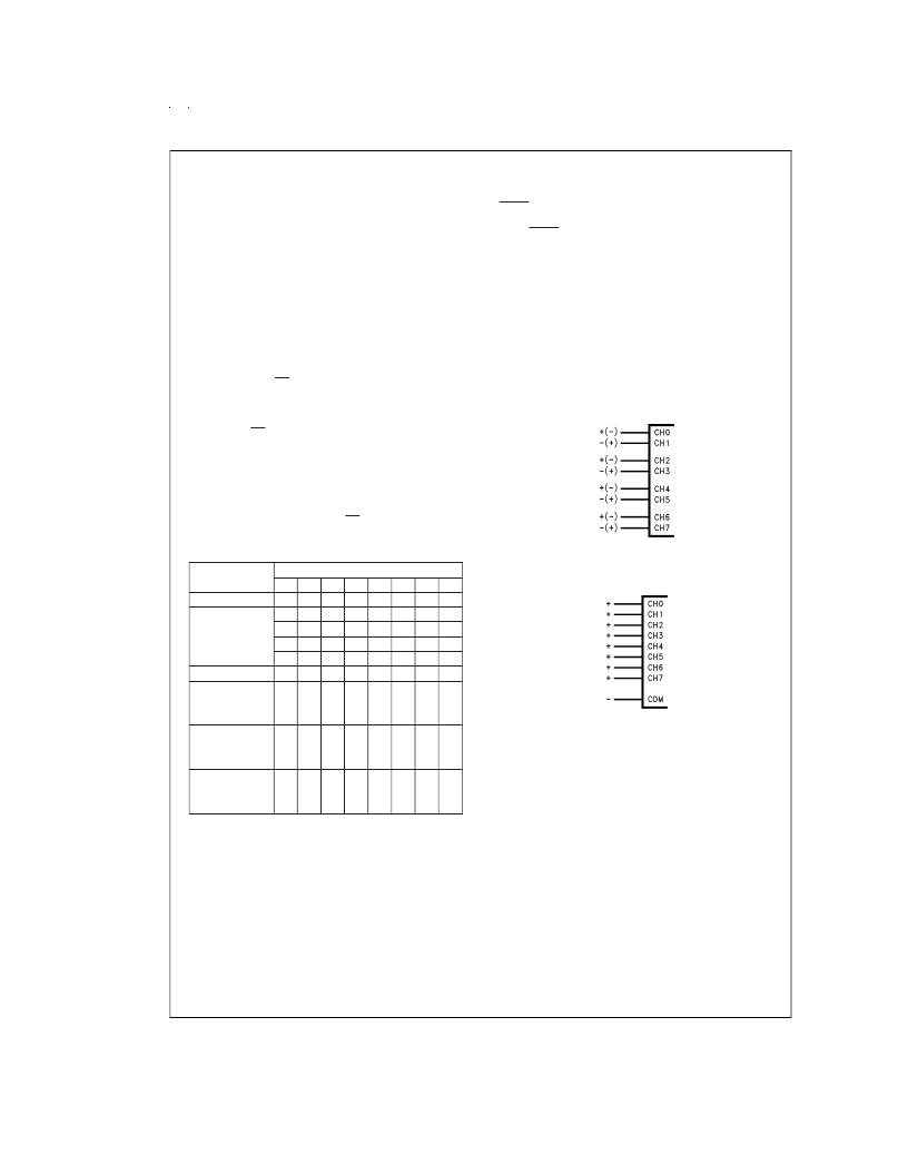
2.0 DESCRIPTION OF THE ANALOG MULTIPLEXER
For the ADC12L038, the analog input multiplexer can be
configured with 4 differential channels or 8 single ended
channels with the COM input as the zero reference or any
combination thereof (see Figure 9 ). The difference between
the voltages on the V
REF+
and V
REF
pins determines the in-
put voltage span (V
). The analog input voltage range is 0
to V
A+
. Negative digital output codes result when V
IN
>
V
IN+
. The actual voltage at V
IN
or V
IN+
cannot go below
AGND.
CH0, CH2, CH4, and CH6 can be assigned to the MUX-
OUT1 pin in the differential configuration, while CH1, CH3,
CH5, and CH7 can be assigned to the MUXOUT2 pin. In the
differential configuration, the analog inputs are paired as fol-
lows: CH0 with CH1, CH2 with CH3, CH4 with CH5 and CH6
with CH7. The A/DIN1 and A/DIN2 pins can be assigned
positive or negative polarity.
With the single-ended multiplexer configuration CH0 through
CH7 can be assigned to the MUXOUT1 pin. The COM pin is
always assigned to the MUXOUT2 pin. A/DIN1 is assigned
as the positive input; A/DIN2 is assigned as the negative in-
put. (See Figure 10 ).
The Multiplexer assignment tables for the ADC12L030,2,4,8
(Tables 2, 3, 4) summarize the aforementioned functions for
the different versions of A/Ds.
4 Differential
Channels
DS011830-38
8 Single-Ended Channels
with COM
as Zero Reference
DS011830-39
FIGURE 9.
www.national.com
26
相關(guān)PDF資料 |
PDF描述 |
|---|---|
| ADC12L038CIWM | 3.3V Self-Calibrating 12-Bit Plus Sign Serial I/O A/D Converters with MUX and Sample/Hold |
| ADC14061CCVT | Self-Calibrating 14-Bit, 2.5 MSPS, 390 mW A/D Converter |
| ADC14061 | Low Dropout Linear 2-cell Li-Ion Charge Controller with AutoCompTM, 8.4V 8-SOIC -20 to 70 |
| ADC14071CIVBH | 14-Bit, 7 MSPS, 380 mW A/D Converter |
| ADC14071 | 14-Bit, 7 MSPS, 380 mW A/D Converter |
相關(guān)代理商/技術(shù)參數(shù) |
參數(shù)描述 |
|---|---|
| ADC12L034CIWMX | 制造商:未知廠家 制造商全稱:未知廠家 功能描述:Single-Ended Data Acquisition System |
| ADC12L038 | 制造商:NSC 制造商全稱:National Semiconductor 功能描述:3.3V Self-Calibrating 12-Bit Plus Sign Serial I/O A/D Converters with MUX and Sample/Hold |
| ADC12L038CIN | 制造商:未知廠家 制造商全稱:未知廠家 功能描述:Single-Ended Data Acquisition System |
| ADC12L038CIWM | 制造商:Rochester Electronics LLC 功能描述:12BIT +SIGN 3.3V SERIAL A/D - Bulk 制造商:Texas Instruments 功能描述: |
| ADC12L038CIWM/NOPB | 功能描述:IC ADC 12BIT W/S&H +SIGN 28SOIC RoHS:是 類別:集成電路 (IC) >> 數(shù)據(jù)采集 - 模數(shù)轉(zhuǎn)換器 系列:- 產(chǎn)品培訓(xùn)模塊:Lead (SnPb) Finish for COTS Obsolescence Mitigation Program 標(biāo)準(zhǔn)包裝:2,500 系列:- 位數(shù):12 采樣率(每秒):3M 數(shù)據(jù)接口:- 轉(zhuǎn)換器數(shù)目:- 功率耗散(最大):- 電壓電源:- 工作溫度:- 安裝類型:表面貼裝 封裝/外殼:SOT-23-6 供應(yīng)商設(shè)備封裝:SOT-23-6 包裝:帶卷 (TR) 輸入數(shù)目和類型:- |
發(fā)布緊急采購,3分鐘左右您將得到回復(fù)。