- 您現(xiàn)在的位置:買賣IC網(wǎng) > PDF目錄378283 > ADC12132CIMSA (NATIONAL SEMICONDUCTOR CORP) Switch-mode Lead-Acid Battery Charger with User-Selectable Charge Algorithms 16-SOIC -20 to 70 PDF資料下載
參數(shù)資料
| 型號(hào): | ADC12132CIMSA |
| 廠商: | NATIONAL SEMICONDUCTOR CORP |
| 元件分類: | ADC |
| 英文描述: | Switch-mode Lead-Acid Battery Charger with User-Selectable Charge Algorithms 16-SOIC -20 to 70 |
| 中文描述: | 2-CH 12-BIT SUCCESSIVE APPROXIMATION ADC, SERIAL ACCESS, PDSO20 |
| 封裝: | SSOP-20 |
| 文件頁(yè)數(shù): | 10/41頁(yè) |
| 文件大小: | 1085K |
| 代理商: | ADC12132CIMSA |
第1頁(yè)第2頁(yè)第3頁(yè)第4頁(yè)第5頁(yè)第6頁(yè)第7頁(yè)第8頁(yè)第9頁(yè)當(dāng)前第10頁(yè)第11頁(yè)第12頁(yè)第13頁(yè)第14頁(yè)第15頁(yè)第16頁(yè)第17頁(yè)第18頁(yè)第19頁(yè)第20頁(yè)第21頁(yè)第22頁(yè)第23頁(yè)第24頁(yè)第25頁(yè)第26頁(yè)第27頁(yè)第28頁(yè)第29頁(yè)第30頁(yè)第31頁(yè)第32頁(yè)第33頁(yè)第34頁(yè)第35頁(yè)第36頁(yè)第37頁(yè)第38頁(yè)第39頁(yè)第40頁(yè)第41頁(yè)
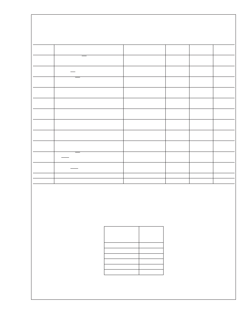
AC Electrical Characteristics
(Continued)
The following specifications apply for (V
+
= V
+ = V
+ = +5V, V
+ = +4.096V, and fully-differential input with fixed 2.048V
common-mode voltage) or (V
+
= V
+ = V
+ = +3.3V, V
+ = +2.5V and fully-differential input with fixed 1.250V
common-mode voltage), V
= 0V, 12-bit + sign conversion mode, source impedance for analog inputs, V
and V
REF
+
≤
25
, f
CK
= f
SK
= 5 MHz, and 10 (t
CK
) acquisition time unless otherwise specified.
Boldface limits apply for T
A
= T
J
=
T
MIN
to T
MAX
;
A
= T
J
= 25C. (Note 17) (Continued)
Symbol
Parameter
Conditions
Typical
(Note 10)
Limits
(Note 11)
50
Units
(Limits)
ns (min)
t
SET-UP
Set-Up Time of CS Falling Edge to
Serial Data Clock Rising Edge
Delay from SCLK Falling
Edge to CS Falling Edge
Delay from CS Rising Edge to
DO TRI-STATE
DI Hold Time from Serial Data
Clock Rising Edge
DI Set-Up Time from Serial Data
Clock Rising Edge
DO Hold Time from Serial Data
Clock Falling Edge
Delay from Serial Data Clock
Falling Edge to DO Data Valid
DO Rise Time, TRI-STATE to High
DO Rise Time, Low to High
DO Fall Time, TRI-STATE to Low
DO Fall Time, High to Low
Delay from CS Falling Edge
to DOR Falling Edge
Delay from Serial Data Clock Falling
Edge to DOR Rising Edge
Capacitance of Logic Inputs
Capacitance of Logic Outputs
t
DELAY
0
5
ns (min)
t
1H
, t
0H
R
L
= 3k, C
L
= 100 pF
70
100
ns (max)
t
HDI
5
15
ns (min)
t
SDI
5
10
ns (min)
t
HDO
R
L
= 3k, C
L
= 100 pF
35
65
5
90
ns (max)
ns (min)
ns (max)
t
DDO
50
t
RDO
R
L
= 3k, C
L
= 100 pF
10
10
15
15
45
40
40
40
40
80
ns (max)
ns (max)
ns (max)
ns (max)
ns (max)
t
FDO
R
L
= 3k, C
L
= 100 pF
t
CD
t
SD
45
80
ns (max)
C
IN
C
OUT
10
20
pF
pF
Note 1:
Absolute Maximum Ratings indicate limits beyond which damage to the device may occur. Operating Ratings indicate conditions for which the device is func-
tional, but do not guarantee specific performance limits. For guaranteed specifications and test conditions, see the Electrical Characteristics. The guaranteed speci-
fications apply only for the test conditions listed. Some performance characteristics may degrade when the device is not operated under the listed test conditions.
Note 2:
All voltages are measured with respect to GND, unless otherwise specified.
Note 3:
When the input voltage (V
IN
) at any pin exceeds the power supplies (V
IN
<
GND or V
IN
>
V
A
+ or V
D
+), the current at that pin should be limited to 30 mA.
The 120 mA maximum package input current rating limits the number of pins that can safely exceed the power supplies with an input current of 30 mA to four.
Note 4:
The maximum power dissipation must be derated at elevated temperatures and is dictated by T
J
max,
θ
JA
and the ambient temperature, T
A
. The maximum
allowable power dissipation at any temperature is P
D
= (T
J
max T
A
)/
θ
JA
or the number given in the Absolute Maximum Ratings, whichever is lower. For this device,
T
J
max = 150C. The typical thermal resistance (
θ
JA
) of these parts when board mounted follow:
Thermal
Resistance
θ
JA
53C/W
70C/W
134C/W
40C/W
50C/W
125C/W
Part Number
ADC12130CIN
ADC12130CIWM
ADC12132CIMSA
ADC12138CIN
ADC12138CIWM
ADC12138CIMSA
Note 5:
The human body model is a 100 pF capacitor discharged through a 1.5 k
resistor into each pin.
Note 6:
See AN450 “Surface Mounting Methods and Their Effect on Product Reliability” or the section titled “Surface Mount” found in any post 1986 National Semi-
conductor Linear Data Book for other methods of soldering surface mount devices.
A
www.national.com
10
相關(guān)PDF資料 |
PDF描述 |
|---|---|
| ADC12138 | Self-Calibrating 12-Bit Plus Sign Serial I/O A/D Converters with MUX and Sample/Hold |
| ADC12130CIN | Self-Calibrating 12-Bit Plus Sign Serial I/O A/D Converters with MUX and Sample/Hold |
| ADC12130CIWM | Self-Calibrating 12-Bit Plus Sign Serial I/O A/D Converters with MUX and Sample/Hold |
| ADC12138CIMSA | Self-Calibrating 12-Bit Plus Sign Serial I/O A/D Converters with MUX and Sample/Hold |
| ADC12138CIN | Self-Calibrating 12-Bit Plus Sign Serial I/O A/D Converters with MUX and Sample/Hold |
相關(guān)代理商/技術(shù)參數(shù) |
參數(shù)描述 |
|---|---|
| ADC12132CIMSA | 制造商:Texas Instruments 功能描述:IC 12BIT ADC SMD 12132 SSOP20 |
| ADC12132CIMSA/NOPB | 制造商:Texas Instruments 功能描述: |
| ADC12132CIMSAX | 功能描述:IC ADC 12BIT 20-SSOP RoHS:是 類別:集成電路 (IC) >> 數(shù)據(jù)采集 - 模數(shù)轉(zhuǎn)換器 系列:- 產(chǎn)品培訓(xùn)模塊:Lead (SnPb) Finish for COTS Obsolescence Mitigation Program 標(biāo)準(zhǔn)包裝:2,500 系列:- 位數(shù):12 采樣率(每秒):3M 數(shù)據(jù)接口:- 轉(zhuǎn)換器數(shù)目:- 功率耗散(最大):- 電壓電源:- 工作溫度:- 安裝類型:表面貼裝 封裝/外殼:SOT-23-6 供應(yīng)商設(shè)備封裝:SOT-23-6 包裝:帶卷 (TR) 輸入數(shù)目和類型:- |
| ADC12138 | 制造商:NSC 制造商全稱:National Semiconductor 功能描述:Self-Calibrating 12-Bit Plus Sign Serial I/O A/D Converters with MUX and Sample/Hold |
| ADC12138CIMSA | 功能描述:模數(shù)轉(zhuǎn)換器 - ADC RoHS:否 制造商:Texas Instruments 通道數(shù)量:2 結(jié)構(gòu):Sigma-Delta 轉(zhuǎn)換速率:125 SPs to 8 KSPs 分辨率:24 bit 輸入類型:Differential 信噪比:107 dB 接口類型:SPI 工作電源電壓:1.7 V to 3.6 V, 2.7 V to 5.25 V 最大工作溫度:+ 85 C 安裝風(fēng)格:SMD/SMT 封裝 / 箱體:VQFN-32 |
發(fā)布緊急采購(gòu),3分鐘左右您將得到回復(fù)。