- 您現(xiàn)在的位置:買賣IC網(wǎng) > PDF目錄10977 > AD9851BRSZRL (Analog Devices Inc)IC SYNTHESR DDS/DAC 28SSOP TR PDF資料下載
參數(shù)資料
| 型號(hào): | AD9851BRSZRL |
| 廠商: | Analog Devices Inc |
| 文件頁(yè)數(shù): | 22/24頁(yè) |
| 文件大小: | 0K |
| 描述: | IC SYNTHESR DDS/DAC 28SSOP TR |
| 產(chǎn)品培訓(xùn)模塊: | Direct Digital Synthesis Tutorial Series (1 of 7): Introduction Direct Digital Synthesizer Tutorial Series (7 of 7): DDS in Action Direct Digital Synthesis Tutorial Series (3 of 7): Angle to Amplitude Converter Direct Digital Synthesis Tutorial Series (6 of 7): SINC Envelope Correction Direct Digital Synthesis Tutorial Series (4 of 7): Digital-to-Analog Converter Direct Digital Synthesis Tutorial Series (2 of 7): The Accumulator |
| 標(biāo)準(zhǔn)包裝: | 1,500 |
| 分辨率(位): | 10 b |
| 主 fclk: | 180MHz |
| 調(diào)節(jié)字寬(位): | 32 b |
| 電源電壓: | 2.7 V ~ 5.25 V |
| 工作溫度: | -40°C ~ 85°C |
| 安裝類型: | 表面貼裝 |
| 封裝/外殼: | 28-SSOP(0.209",5.30mm 寬) |
| 供應(yīng)商設(shè)備封裝: | 28-SSOP |
| 包裝: | 帶卷 (TR) |
第1頁(yè)第2頁(yè)第3頁(yè)第4頁(yè)第5頁(yè)第6頁(yè)第7頁(yè)第8頁(yè)第9頁(yè)第10頁(yè)第11頁(yè)第12頁(yè)第13頁(yè)第14頁(yè)第15頁(yè)第16頁(yè)第17頁(yè)第18頁(yè)第19頁(yè)第20頁(yè)第21頁(yè)當(dāng)前第22頁(yè)第23頁(yè)第24頁(yè)
AD9851
–7–
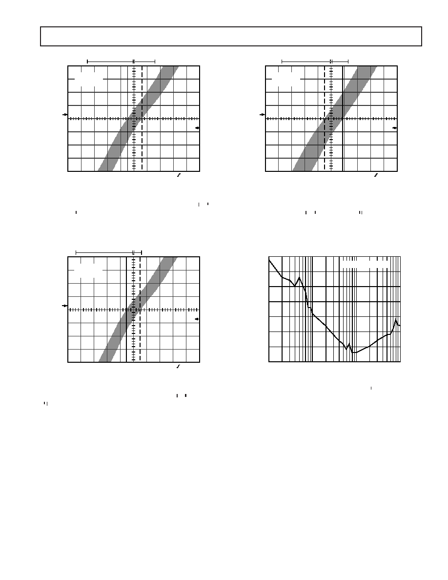
1
Ch1 200mV
T [
]
Tek Run 4.00GS/s
Sample
M 12.5ns Ch 1
–200mV
D 200ps Runs After
: 208ps
@ : 1.940ns
TPC 7. Typical CMOS comparator p-p output jitter with
the AD9851 configured as a clock generator, DDS fOUT
the AD9851 configured as a clock generator, DDS f
=
OUT
10.1 MHz, VS
10.1 MHz, V
10.1 MHz, V = 5 V, system clock = 180 MHz, 70 MHz LPF.
S
Graph details the center portion of a rising edge with
scope in delayed trigger mode, 200 ps/div. Cursors show
208 ps p-p jitter.
1
Ch1 200mV
T
[
]
Tek Run 4.00GS/s
Sample
M 12.5ns Ch 1
–200mV
D 200ps Runs After
: 204ps
@ : 3.672ns
TPC 8. Typical CMOS comparator p-p output jitter with the
AD9851 configured as a clock generator, DDS fOUT
AD9851 configured as a clock generator, DDS f
= 40.1 MHz,
OUT
VS
V
V = 5 V, system clock = 180 MHz, 70 MHz LPF. Graph details
S
the center portion of a rising edge with scope in delayed
trigger mode, 200 ps/div. Cursors show 204 ps p-p jitter.
1
Ch1 200mV
T
[
]
Tek Run 4.00GS/s
Sample
: 280ps
@ : 2.668ns
M 12.5ns Ch 1
–200mV
D 200ps Runs After
TPC 9. Typical CMOS comparator p-p output
jitter with the AD9851 configured as a clock
generator, DDS fOUT
generator, DDS f
= 70.1 MHz, V
OUT
S
= 70.1 MHz, V
= 70.1 MHz, V = 5 V, system
S
clock = 180 MHz, 70 MHz LPF. Graph details
the center portion of a rising edge with scope
in delayed trigger mode, 200 ps/div. Cursors
show 280 ps p-p jitter.
FREQUENCY OFFSET – Hz
–145
100
MAGNITUDE
–
dBc/Hz
1k
10k
100k
–135
–130
–125
–120
–115
–100
AD9851 PHASE NOISE
–140
TPC 10. Output Phase Noise (5.2 MHz AOUT), 6
OUT
REFCLK
Multiplier Enabled, System Clock = 180 MHz, Reference
Clock = 30 MHz
REV. D
相關(guān)PDF資料 |
PDF描述 |
|---|---|
| VE-BW3-IY-F3 | CONVERTER MOD DC/DC 24V 50W |
| VE-BW2-IY-F3 | CONVERTER MOD DC/DC 15V 50W |
| AD9850BRSZ-REEL | IC DDS SYNTHESIZER CMOS 28-SSOP |
| VE-BW1-IY-F2 | CONVERTER MOD DC/DC 12V 50W |
| VE-BW0-IY-F2 | CONVERTER MOD DC/DC 5V 50W |
相關(guān)代理商/技術(shù)參數(shù) |
參數(shù)描述 |
|---|---|
| AD9851CGPCB | 制造商:AD 制造商全稱:Analog Devices 功能描述:CMOS 180 MHz DDS/DAC Synthesizer |
| AD9851FSPCB | 制造商:Analog Devices 功能描述:EVALUATION BOARD ((NS)) |
| AD9852 | 制造商:AD 制造商全稱:Analog Devices 功能描述:CMOS 300 MHz Complete-DDS |
| AD9852/PCB | 制造商:Analog Devices 功能描述:NCO, CMOS 300MSPS COMPLETE-DDS |
| AD9852/PCBZ | 功能描述:BOARD EVAL FOR AD9852 RoHS:是 類別:RF/IF 和 RFID >> RF 評(píng)估和開發(fā)套件,板 系列:AgileRF™ 標(biāo)準(zhǔn)包裝:1 系列:- 類型:GPS 接收器 頻率:1575MHz 適用于相關(guān)產(chǎn)品:- 已供物品:模塊 其它名稱:SER3796 |
發(fā)布緊急采購(gòu),3分鐘左右您將得到回復(fù)。