- 您現(xiàn)在的位置:買賣IC網(wǎng) > PDF目錄373968 > AD9844 (Analog Devices, Inc.) Complete 12-Bit 20 MSPS CCD Signal Processor PDF資料下載
參數(shù)資料
| 型號: | AD9844 |
| 廠商: | Analog Devices, Inc. |
| 英文描述: | Complete 12-Bit 20 MSPS CCD Signal Processor |
| 中文描述: | 完整的12位20 MSPS的CCD信號處理器 |
| 文件頁數(shù): | 15/16頁 |
| 文件大小: | 169K |
| 代理商: | AD9844 |
AD9844A
–15–
REV. 0
CCD
CCDIN
BUFFER
V
OUT
0.1 F
ADC
OUT
REGISTER
DATA
SERIAL
INTERFACE
DIGITAL
OUTPUTS
DIGITAL IMAGE
PROCESSING
ASIC
TIMING
GENERATOR
V-DRIVE
CCD
TIMING
CDS/CLAMP
TIMING
AD9844A
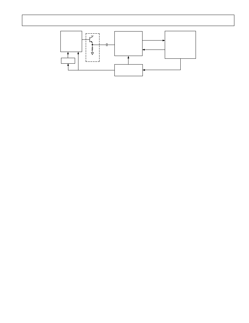
Figure 16. System Applications Diagram
APPLICATIONS INFORMATION
The AD9844A is a complete Analog Front End (AFE) product
for digital still camera and camcorder applications. As shown in
Figure 16, the CCD image (pixel) data is buffered and sent to
the AD9844A analog input through a series input capacitor. The
AD9844A performs the dc restoration, CDS, gain adjustment,
black level correction, and analog-to-digital conversion. The
AD9844A’s digital output data is then processed by the image
processing ASIC. The internal registers of the AD9844A—used to
control gain, offset level, and other functions—are programmed
by the ASIC or microprocessor through a 3-wire serial digital
interface. A system timing generator provides the clock signals
for both the CCD and the AFE.
Internal Power-On Reset Circuitry
After power-on, the AD9844A will automatically reset all inter-
nal registers and perform internal calibration procedures. This
takes approximately 1 ms to complete. During this time, normal
clock signals and serial write operations may occur. However,
serial register writes will be ignored until the internal reset opera-
tion is completed. Pin 43 (formerly RSTB on the AD9843
non-A) is no longer used for the reset operation. Toggling Pin
43 in the AD9844A will have no effect.
Grounding and Decoupling Recommendations
As shown in Figure 17, a single ground plane is recommended
for the AD9844A. This ground plane should be as continu-
ous as possible, particularly around Pins 25 through 39. This will
ensure that all analog decoupling capacitors provide the lowest
possible impedance path between the power and bypass pins
and their respective ground pins. All decoupling capacitors
should be located as close as possible to the package pins. A
single clean power supply is recommended for the AD9844A, but
a separate digital driver supply may be used for DRVDD (Pin
13). DRVDD should always be decoupled to DRVSS (Pin 14),
which should be connected to the analog ground plane. Advan-
tages of using a separate digital driver supply include using a
lower voltage (2.7 V) to match levels with a 2.7 V ASIC, reducing
digital power dissipation, and reducing potential noise coupling.
If the digital outputs (Pins 3–12) must drive a load larger than
20 pF, buffering is recommended to reduce digital code transi-
tion noise. Alternatively, placing series resistors close to the
digital output pins may help reduce noise.
相關(guān)PDF資料 |
PDF描述 |
|---|---|
| AD9844A | Complete 12-Bit 20 MSPS CCD Signal Processor |
| AD9844AJST | Complete 12-Bit 20 MSPS CCD Signal Processor |
| AD9845B | Complete 12-Bit 30 MSPS CCD Signal Processor |
| AD9845BJST | Complete 12-Bit 30 MSPS CCD Signal Processor |
| AD9845 | Complete 12-Bit 30 MSPS CCD Signal Processor |
相關(guān)代理商/技術(shù)參數(shù) |
參數(shù)描述 |
|---|---|
| AD9844A | 制造商:AD 制造商全稱:Analog Devices 功能描述:Complete 12-Bit 20 MSPS CCD Signal Processor |
| AD9844AJST | 制造商:Analog Devices 功能描述:AFE Video 1ADC 12-Bit 3.3V 48-Pin LQFP 制造商:Analog Devices 功能描述:AFE VID 1ADC 12-BIT 3.3V 48LQFP - Bulk 制造商:Rochester Electronics LLC 功能描述:12 BIT 20 MHZ ANALOG FRONT END - Tape and Reel |
| AD9844AJSTRL | 制造商:Analog Devices 功能描述:AFE Video 1ADC 12-Bit 3.3V 48-Pin LQFP T/R 制造商:Analog Devices 功能描述:AFE VID 1ADC 12-BIT 3.3V 48LQFP - Tape and Reel 制造商:Rochester Electronics LLC 功能描述:12 BIT 20 MHZ ANALOG FRONT END - Tape and Reel |
| AD9844AJSTZ | 制造商:Analog Devices 功能描述:AFE Video 1ADC 12-Bit 3.3V 48-Pin LQFP 制造商:Analog Devices 功能描述:12 BIT 20 MHz ANALOG FRONT END |
| AD9844-EB | 制造商:Analog Devices 功能描述: |
發(fā)布緊急采購,3分鐘左右您將得到回復(fù)。