- 您現(xiàn)在的位置:買賣IC網(wǎng) > PDF目錄373968 > AD9816 (Analog Devices, Inc.) Complete 12-Bit 6 MSPS CCD/CIS Signal Processor(12位的采樣速率為6MSPS的CCD/CIS信號(hào)處理器) PDF資料下載
參數(shù)資料
| 型號(hào): | AD9816 |
| 廠商: | Analog Devices, Inc. |
| 英文描述: | Complete 12-Bit 6 MSPS CCD/CIS Signal Processor(12位的采樣速率為6MSPS的CCD/CIS信號(hào)處理器) |
| 中文描述: | 完整的12位6 MSPS的防治荒漠化公約/ CIS信號(hào)處理器(12位的采樣速率為6MSPS的防治荒漠化公約/獨(dú)聯(lián)體信號(hào)處理器) |
| 文件頁數(shù): | 12/16頁 |
| 文件大?。?/td> | 190K |
| 代理商: | AD9816 |
AD9816
–12–
REV. A
Line Clamp
If a line clamp technique is implemented (see Figure 5 for
timing), the value of C
IN
should be increased to more than
1200 pF. The main requirement for line clamp is to keep the
signal droop below 1 LSB across a scanned line. For example, if
a CCD with 5400 effective pixels is clocked at 2 MHz, then
t = 2.7 ms. One LSB at 12 bits with a 3 V full scale is 732
μ
V.
Rearranging the above droop equation:
C
MIN
=
i
BIAS
dV
×
t
In this case, C
MIN
= 37 nF, and a convenient standard value of
0.047
μ
F will be adequate.
SHA Mode Operation
When the AD9816 is configured for SHA mode operation, the
OFFSET pin functions as an offset adjustment input. Figure
15 shows a simplified diagram of the AD9816’s inputs when SHA
mode is selected. A positive dc voltage may be applied to OFFSET
which will be subtracted from all three input channels in the
input stage of the AD9816. The maximum input voltage to the
analog input pins or the OFFSET pin in SHA mode is 3 V.
The OFFSET feature is provided to allow coarse offset adjust-
ment of the input signal. If the signal is sampled with respect to
ground, any positive offset on the input signal will subtract from
the dynamic range of the ADC. For example, an input signal
that spans from 1.5 V to 2.5 V cannot utilize all of the available
dynamic range, using either the 1.5 V or 3 V span. However, by
applying a dc value of 1.5 V to the OFFSET pin, the input
signal will be level-shifted down to 0 V to 1 V. This would
allow the use of the 3 V span and a PGA gain of three to use
the entire ADC dynamic range.
If no dc offset adjustment is desired, the OFFSET pin should
be grounded. The input signal will be sampled with respect to
ground.
SHA
BUFFER
SHA
BUFFER
SHA
BUFFER
VINR
VING
VINB
OFFSET
AD9816
CDSCLK1
CDSCLK2
12k
V
Figure 15. SHA Mode Input Circuit
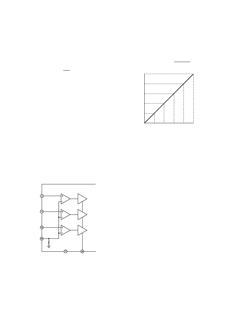
Programmable Gain Amplifiers
The AD9816 has three programmable amplifiers, one for each
channel. The gain is variable from 1 V/V (0 dB) to 5.98 V/V
(15.5 dB) in 256 increments. Figure 16 shows the PGA gain
transfer function. The gain of the PGA can be calculated ac-
cording to the equation:
PGAGain
=
1
+
Gain Code
51.2
GAIN REGISTER CODE – Decimal
P
6
5
1
0
51
255
102
153
204
4
3
2
Figure 16. PGA Gain Transfer Function
The analog outputs of the three PGAs are multiplexed to the input
of the 12-bit ADC. The differential output of the MUX is also
buffered and externally available at Pins 43 and 44 (PGAOUT_C
and PGAOUT_T, respectively). The timing diagrams, Fig-
ures 1 through 4, show the timing relationships between the
analog inputs, CDSCLK2, ADCCLK, and PGAOUT_T and
PGAOUT_C. The CDSCLK2 pulse resets the outputs of all
three PGAs to an internal bias level. The first rising edge of
ADCCLK after the rising edge of CDSCLK2 will switch the
MUX to the red PGA output. The second ADCCLK rising
edge switches the MUX to the green PGA output, and the third
rising edge switches the MUX to the blue PGA output.
PGA Outputs
The PGAOUT_T and PGAOUT_C signals represent the differ-
ential input to the ADC, and are complementary. Both signals
will reset to 3.5 V while CDSCLK2 is high. The voltage swing
of each output is equal to one-half of the ADC’s full-scale volt-
age, centered at 3.5 V. Table V shows the relationship between
the analog input voltage, the PGA output voltage and the ADC
input voltage.
Figure 18 shows the PGA output voltages for three different
color pixel amplitudes. In this example, the red pixel has the
largest amplitude, and the blue pixel has the smallest amplitude.
Because the PGAOUT_T and PGAOUT_C outputs are inter-
nally buffered by source followers, they are not an exact repre-
sentation of the differential ADC input signal. PGAOUT_T and
PGAOUT_C should only be used during evaluation; perfor-
mance of the AD9816 is only guaranteed with these two pins
unconnected.
相關(guān)PDF資料 |
PDF描述 |
|---|---|
| AD9821 | Complete 12-Bit 40 MSPS Imaging Signal Processor |
| AD9821KST | Complete 12-Bit 40 MSPS Imaging Signal Processor |
| AD9822 | Complete 14-Bit CCD/CIS Signal Processor |
| AD9822JR | Complete 14-Bit CCD/CIS Signal Processor |
| AD9822JRS | Complete 14-Bit CCD/CIS Signal Processor |
相關(guān)代理商/技術(shù)參數(shù) |
參數(shù)描述 |
|---|---|
| AD9816-EB | 制造商:Analog Devices 功能描述:12-BIT 4MSPS CCD/CIS SIGNAL PROCESSOR - Bulk |
| AD9816JS | 制造商:Analog Devices 功能描述:AFE VID 1ADC 12-BIT 5V/5V 44MQFP - Bulk 制造商:Rochester Electronics LLC 功能描述: |
| AD9816JS-80010 | 制造商:AD 制造商全稱:Analog Devices 功能描述:Complete 12-Bit 6 MSPS CCD/CIS Signal Processor |
| AD9816JSRL | 制造商:Rochester Electronics LLC 功能描述:- Tape and Reel 制造商:Analog Devices 功能描述: |
| AD9821 | 制造商:AD 制造商全稱:Analog Devices 功能描述:Complete 12-Bit 40 MSPS Imaging Signal Processor |
發(fā)布緊急采購,3分鐘左右您將得到回復(fù)。