- 您現(xiàn)在的位置:買賣IC網(wǎng) > PDF目錄373968 > AD9802JST (ANALOG DEVICES INC) Silver Mica Capacitor; Capacitance:10pF; Capacitance Tolerance: 5%; Series:CD17; Voltage Rating:500VDC; Capacitor Dielectric Material:Mica; Termination:Radial Leaded; Lead Pitch:5.9mm; Leaded Process Compatible:Yes RoHS Compliant: Yes PDF資料下載
參數(shù)資料
| 型號: | AD9802JST |
| 廠商: | ANALOG DEVICES INC |
| 元件分類: | 消費家電 |
| 英文描述: | Silver Mica Capacitor; Capacitance:10pF; Capacitance Tolerance: 5%; Series:CD17; Voltage Rating:500VDC; Capacitor Dielectric Material:Mica; Termination:Radial Leaded; Lead Pitch:5.9mm; Leaded Process Compatible:Yes RoHS Compliant: Yes |
| 中文描述: | SPECIALTY CONSUMER CIRCUIT, PQFP48 |
| 封裝: | PLASTIC, TQFP-48 |
| 文件頁數(shù): | 10/20頁 |
| 文件大?。?/td> | 366K |
| 代理商: | AD9802JST |
AD9802
–10–
REV. 0
APPLICAT IONS INFORMAT ION
Generating Clock Signals
For best performance, the AD9802 should be driven by 3 V
logic levels. As shown in the Equivalent Input Circuits, the use
of 5 V logic for ADCCLK will turn on the protection diode to
DVDD, increasing the current flow into this pin. As a result,
noise and power dissipation will increase. T he CDS clock in-
puts, SHP and SHD, have a additional protection and can with-
stand direct 5 V levels.
External clamping diodes or resistor dividers can be used to
translate 5 V levels to 3 V levels, but the lowest power dissi-
pation is achieved with a logic transceiver chip. National
Semiconductor’s 74LVX 4245 provides a 5 V to 3 V level shift
for up to eight clock signals, has a three-state option, and
features low power consumption. Philips Semiconductor and
Quality also manufacture similar devices.
Driving the Direct ADC Input
T he AD9802 can be used in a “direct ADC input” mode, in
which the input signal bypasses the input clamp, CDS and
PGA, and is sent directly to the sample and hold amplifier (SHA)
of the ADC. T here are several methods that may be used to
drive the direct ADC input.
T o enable the direct input mode of operation, ADCMODE (Pin
41) is taken to logic high. T his will internally disconnect the
PGA output from the SHA input, and connect ADCIN (Pin 36)
to the SHA input.
T he SHA has a differential input, consisting of ADCIN (Pin 36)
as the positive input, and SHABYP (Pin 38) as the negative
input. Both pins must be properly dc biased.
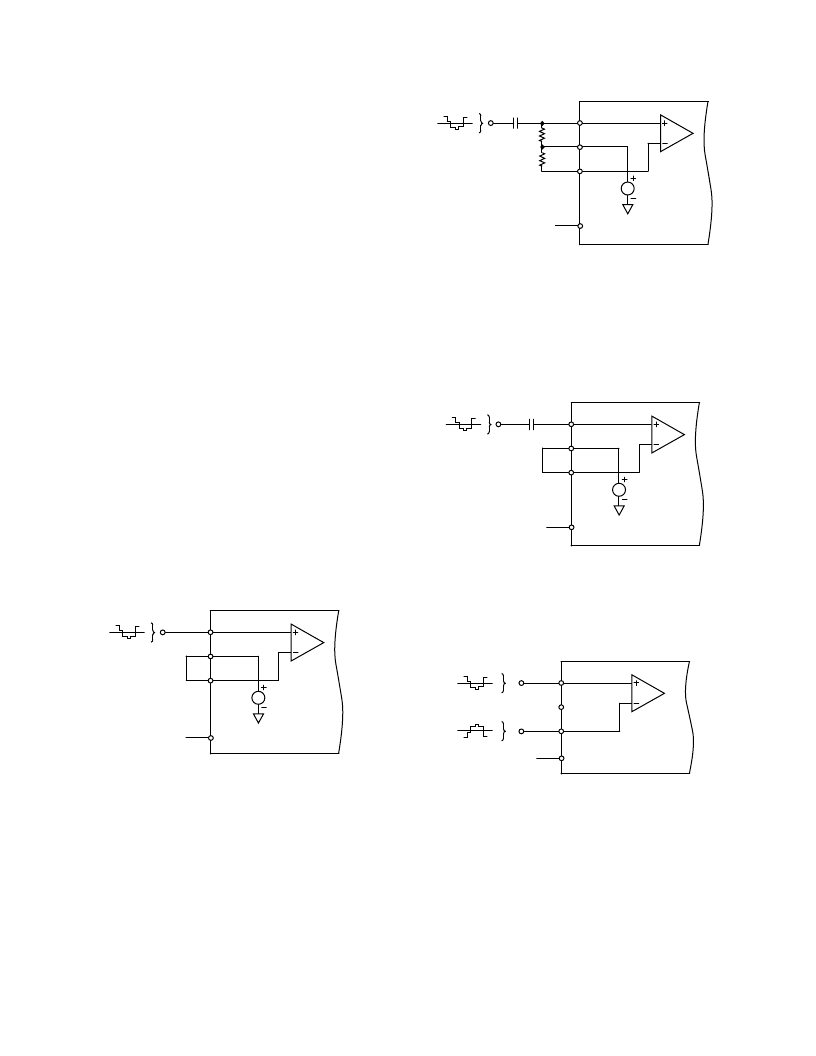
Figures 22 through 25 show four circuits for driving the direct
ADC input. Decoupling capacitors are not shown for CML,
VRT , VRB and SHABYP pins.
SHA
ADCIN
CML
SHABYP
1.5V
1V p-p
CML
+3V
ADCMODE
AD9802
Figure 22. DC-Coupled Input
Figure 22 is a single-ended, dc-coupled circuit. SHABYP is
connected to CML (1.5 V) to establish a midpoint bias. T he
input signal of 1 V p-p should be centered around CML.
Figure 23 shows an ac-coupled configuration, where both inputs
are biased to CML. T he input capacitor C
IN
and bias resistors
should be sized to set the appropriate high pass cutoff frequency
for the application. T o minimize the differential offset voltage
due to the input bias currents, both resistors should be equal.
SHA
ADCIN
CML
SHABYP
1.5V
1V p-p
+3V
ADCMODE
AD9802
R
BIAS
R
BIAS
C
IN
Figure 23. AC-Coupled Input
Figure 24 shows an alternative ac-coupled configuration. By
connecting SHABYP to CML, the dc bias at Pin 36 (ADCIN)
will internally track to the same voltage, automatically setting
the input bias level. With a given input capacitor value, C
IN
, the
time constant in this configuration will be dependent on the
sampling frequency F
S
. Specifically:
τ
= (
C
IN
/
F
S
)
×
2
E
+12
SHA
ADCIN
CML
SHABYP
1.5V
1V p-p
+3V
ADCMODE
AD9802
C
IN
Figure 24. “ Auto Bias” AC-Coupled Input
Figure 25 shows a true differential drive circuit. Each input
would be 500 mV p-p, to achieve the 1 V full-scale input to the
ADC. T he common-mode input range for this configuration
extends from about 500 mV to 2.5 V. T his circuit could also be
implemented with ac coupling, similar to Figure 23.
SHA
ADCIN
CML
SHABYP
500mV p-p
+3V
ADCMODE
AD9802
500mV p-p
Figure 25. Differential Input
Figure 26 shows a video clamp circuit which may be used with
the direct ADC mode of the AD9802 (supplies and decoupling
not shown). T he circuit will clamp the reference black level of
an incoming video signal to 1.25 V dc. With SHABYP con-
nected to 1.75 V (VRT ), the ADCIN range spans from 1.25 V
to 2.25 V. T o accomplish this, the CLAMP pulse should be
asserted during the horizontal sync interval, when the video is at
its reference black level. A 5 V logic high applied to the gate of
the SD210 will turn on the device, and the input capacitor C
IN
will charge up to provide 1.25 V at the ADCIN pin of the
AD9802. Other appropriate NMOS devices may be substituted
for the SD210. T he AD8047 op amp requires
±
5 V supplies;
appropriate single supply op amps may be substituted. T he size
of capacitor C
IN
should be set to meet the acquisition time and
相關(guān)PDF資料 |
PDF描述 |
|---|---|
| AD9802 | .50" x 50 Black/Clear 240 Industrial Label Supply RoHS Compliant: NA |
| AD9803 | CCD And Video Signal Processor For Electronic Cameras(電子照相機的CCD信號和視頻信號處理器) |
| AD9805 | Complete 12-Bit/10-Bit 6 MSPS CCD/CIS Signal Processors |
| AD9805JS | Complete 12-Bit/10-Bit 6 MSPS CCD/CIS Signal Processors |
| AD9807 | Complete 12-Bit/10-Bit 6 MSPS CCD/CIS Signal Processors |
相關(guān)代理商/技術(shù)參數(shù) |
參數(shù)描述 |
|---|---|
| AD9802JSTRL | 制造商:Rochester Electronics LLC 功能描述:- Tape and Reel |
| AD9803 | 制造商:AD 制造商全稱:Analog Devices 功能描述:CCD Signal Processor For Electronic Cameras |
| AD9803JST | 制造商:Rochester Electronics LLC 功能描述: |
| AD9803JST-28 | 制造商:Rochester Electronics LLC 功能描述:- Bulk |
| AD9803JSTRL-28 | 制造商:Rochester Electronics LLC 功能描述:- Bulk |
發(fā)布緊急采購,3分鐘左右您將得到回復(fù)。