- 您現(xiàn)在的位置:買賣IC網(wǎng) > PDF目錄362110 > AD840JQ (ANALOG DEVICES INC) Wideband, Fast Settling Op Amp PDF資料下載
參數(shù)資料
| 型號: | AD840JQ |
| 廠商: | ANALOG DEVICES INC |
| 元件分類: | 運(yùn)動(dòng)控制電子 |
| 英文描述: | Wideband, Fast Settling Op Amp |
| 中文描述: | OP-AMP, 1500 uV OFFSET-MAX, 400 MHz BAND WIDTH, CDIP14 |
| 封裝: | HERMETIC SEALED, CERDIP-14 |
| 文件頁數(shù): | 13/20頁 |
| 文件大?。?/td> | 463K |
| 代理商: | AD840JQ |
REV. C
AD8400/AD8402/AD8403
–13–
OPERATION
The AD8400/AD8402/AD8403 provide a single, dual, and quad
channel, 256-position digitally controlled variable resistor (VR)
device. Changing the programmed VR settings is accomplished by
clocking in a 10-bit serial data word into the SDI (Serial Data Input)
pin. The format of this data word is two address bits, MSB first,
followed by eight data bits, MSB first. Table I provides the serial
register data word format. The AD8400/AD8402/AD8403 has the
following address assignments for the ADDR decode, which
determines the location of VR latch receiving the serial register
data in Bits B7 through B0:
VR
A
A
#
=
×
+
+
1
2
0
1
(1)
The single-channel AD8400 requires A1 = A0 = 0. The dual-
channel AD8402 requires A1 = 0. VR settings can be changed
one at a time in random sequence. The serial clock running at
10 MHz makes it possible to load all four VRs in under 4
μ
s
(10
×
4
×
100 ns) for the AD8403. The exact timing requirements
are shown in Figures 2a, 2b, and 2c.
The AD8402/AD8403 resets to midscale by asserting the
RS
pin, simplifying initial conditions at power up. Both parts have a
power shutdown
SHDN
pin that places the VR in a zero power
consumption state where terminals Ax are open circuited and the
wiper Wx is connected to Bx resulting in only leakage currents
being consumed in the VR structure. In shutdown mode the VR
latch settings are maintained so that returning to operational mode
from power shutdown, the VR settings return to their previous
resistance values. The digital interface is still active in shutdown,
except that SDO is deactivated. Code changes in the registers can
be made that will produce new wiper positions when the device is
taken out of shutdown.
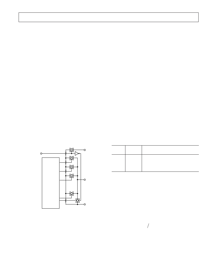
D7
D6
D5
D4
D3
D2
D1
D0
RDAC
LATCH
AND
DECODER
Ax
Wx
Bx
R
S
= R
NOMINAL
/256
R
S
R
S
R
S
R
S
SHDN
Figure 3. AD8402/AD8403 Equivalent VR (RDAC) Circuit
PROGRAMMING THE VARIABLE RESISTOR
Rheostat Operation
The nominal resistance of the VR (RDAC) between terminals A and
B is available with values of 1 k
, 10 k
, 50 k
, and 100 k
. The
final digits of the part number determine the nominal resistance
value, e.g., 10 k
= 10; 100 k
= 100. The nominal resistance
(R
AB
) of the VR has 256 contact points accessed by the wiper
terminal, plus the B terminal contact. The 8-bit data word in the
RDAC latch is decoded to select one of the 256 possible settings.
The wiper
’
s first connection starts at the B terminal for data 00
H
.
This B terminal connection has a wiper contact resistance of 50
.
The second connection (10 k
part) is the first tap point located
at 89
[= R
AB
(nominal resistance)/256 + R
W
= 39
+ 50
] for
data 01
H
. The third connection is the next tap point representing
78 + 50 = 128
for data 02
H
. Each LSB data value increase
moves the wiper up the resistor ladder until the last tap point is
reached at 10,011
. The wiper does not directly connect to the
B terminal. See Figure 3 for a simplified diagram of the equiva-
lent RDAC circuit.
The AD8400 contains one RDAC, the AD8402 contains two
independent RDACs, and the AD8403 contains four independent
RDACs. The general transfer equation that determines the digi-
tally programmed output resistance between Wx and Bx is:
(
/ 256
where
Dx
is the data contained in the 8-bit RDAC# latch, and
R
AB
is the nominal end-to-end resistance.
For example, when V
B
= 0 V and when the A terminal is open
circuit, the following output resistance values will be set for the
following RDAC latch codes (applies to 10 k
potentiometers):
R
Dx
Dx
R
R
WB
AB
W
)
=
(
)
×
+
(2)
D
(Dec)
R
WB
( )
Output State
255
128
1
0
10,011
5,050
89
50
Full Scale
Midscale (
RS
= 0 Condition)
1 LSB
Zero-Scale (Wiper Contact Resistance)
Note in the zero-scale condition a finite wiper resistance of 50
is present. Care should be taken to limit the current flow between
W and B in this state to a maximum value of 5 mA to avoid
degradation or possible destruction of the internal switch contact.
Like the mechanical potentiometer the RDAC replaces, it is totally
symmetrical. The resistance between the wiper W and terminal
A also produces a digitally controlled complementary resistance
R
WA
. When these terminals are used, the B terminal can be tied
to the wiper or left floating. Setting the resistance value for R
WA
starts at a maximum value of resistance and decreases as the data
loaded in the RDAC latch is increased in value. The general transfer
equation for this operation is:
(
256
256
R
D
D
R
R
WA
X
X
AB
W
)
=
(
)
×
+
(3)
相關(guān)PDF資料 |
PDF描述 |
|---|---|
| AD840KN | Wideband, Fast Settling Op Amp |
| AD840KQ | Wideband, Fast Settling Op Amp |
| AD842* | Wideband. High Output Current. Fast Settling Op Amp |
| AD842SE | Voltage-Feedback Operational Amplifier |
| AD842JH | Wideband, High Output Current, Fast Settling Op Amp |
相關(guān)代理商/技術(shù)參數(shù) |
參數(shù)描述 |
|---|---|
| AD840KN | 制造商:Rochester Electronics LLC 功能描述:- Bulk 制造商:Analog Devices 功能描述: |
| AD840KQ | 制造商:AD 制造商全稱:Analog Devices 功能描述:Wideband, Fast Settling Op Amp |
| AD840S | 制造商: 功能描述: 制造商:undefined 功能描述: |
| AD840SE/883B | 制造商:Rochester Electronics LLC 功能描述:PRECISION HIGH SPEED AMP - Bulk |
| AD840SE-883B | 制造商:AD 制造商全稱:Analog Devices 功能描述:Wideband, Fast Settling Op Amp |
發(fā)布緊急采購,3分鐘左右您將得到回復(fù)。