- 您現(xiàn)在的位置:買賣IC網(wǎng) > PDF目錄373916 > AD7751ABRS (ANALOG DEVICES INC) ECONOLINE: RB & RA - Dual Output from a Single Input Rail- Power Sharing on Output- Industry Standard Pinout- 1kVDC & 2kVDC Isolation- Custom Solutions Available- UL94V-0 Package Material- Efficiency to 85% PDF資料下載
參數(shù)資料
| 型號: | AD7751ABRS |
| 廠商: | ANALOG DEVICES INC |
| 元件分類: | 模擬信號調(diào)理 |
| 英文描述: | ECONOLINE: RB & RA - Dual Output from a Single Input Rail- Power Sharing on Output- Industry Standard Pinout- 1kVDC & 2kVDC Isolation- Custom Solutions Available- UL94V-0 Package Material- Efficiency to 85% |
| 中文描述: | SPECIALTY ANALOG CIRCUIT, PDSO24 |
| 封裝: | SSOP-24 |
| 文件頁數(shù): | 14/16頁 |
| 文件大?。?/td> | 249K |
| 代理商: | AD7751ABRS |
REV. A
AD7751
–14–
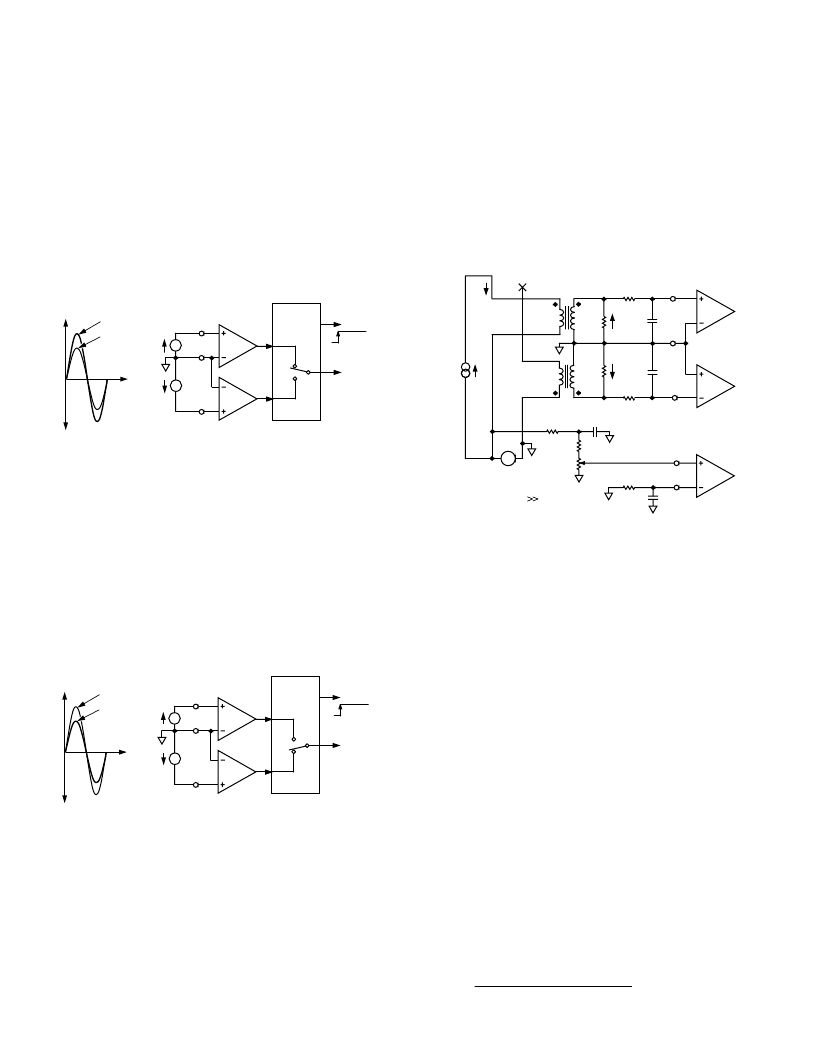
Fault with Active Input Greater than Inactive Input
If V1A is the active current input (i.e., is being used for billing),
and the signal on V1B (inactive input) falls by more than 12.5%
of V1A, the fault indicator will go active. Both analog inputs are
filtered and averaged to prevent false triggering of this logic
output. As a consequence of the filtering, there is a time delay of
approximately one second on the logic output FAULT after the
fault event. The FAULT logic output is independent of any activ-
ity on outputs F1 or F2. Figure 13 illustrates one condition under
which FAULT becomes active. Since V1A is the active input and it
is still greater than V1B, billing is maintained on VIA, i.e., no swap
to the V1B input will occur. V1A remains the active input.
V1B < 87.5% OF V1A
0V
V1A
V1B
V1A
V1A
V1N
AGND
V1B
V1B
FILTER
AND
COMPARE
TO
MULTIPLIER
FAULT
A
B
Figure 13. Fault Conditions for Inactive Input Less than
Active Input
Fault with V1B Greater than V1A
Figure 14 illustrates another fault condition. If V1A is the active
input (i.e., is being used for billing), and the voltage signal on
V1B (inactive input) becomes greater than 114% of V1A, the
FAULT indicator goes active and there is also a swap over to
the V1B input. The analog input V1B has now become the
active input. Again there is a time delay of about 1.2 second
associated with this swap. V1A will not swap back to being the
active channel until V1A becomes greater than 114% of V1B.
However, the FAULT indicator will become inactive as soon as
V1A is within 12.5% of V1B. This threshold eliminates poten-
tial chatter between V1A and V1B.
V1A < 87.5% OF V1B
OR
V1B > 114% OF V1A
0V
V1A
V1B
V1A
V1A
V1N
AGND
V1B
V1B
FILTER
AND
COMPARE
TO
MULTIPLIER
FAULT
A
B
Figure 14. Fault Conditions for Inactive Input Greater than
Active Input
Calibration Concerns
Typically, when a meter is being calibrated, the voltage and current
circuits are separated as shown in Figure 15. This means that
current will only pass through the phase or neutral circuit. Figure
15 shows current being passed through the phase circuit. This is
the preferred option since the AD7751 starts billing on the input
V1A on power-up. The phase circuit CT is connected to V1A in
the diagram. Since there is no current in the neutral circuit the
FAULT indicator will come on under these conditions. However,
this does not affect the accuracy of the calibration and can be
used as a means to test the functionality of the fault detection.
Ib
V
240Vrms
NOTE:
Ra
Rb + VR = R
f
R
;
Rb
Rb
V1A
0V
V1B
CT
V1A
AGND
R
f
CT
NEUTRAL
PHASE
V1N
C
f
C
f
R
f
Rb
VR
V2P
R
f
V2N
C
f
C
f
TEST
CURRENT
Ib
Ra
Figure 15. Fault Conditions for Inactive Input Greater than
Active Input
If the neutral circuit is chosen for the current circuit in the arrange-
ment shown in Figure 15, it may have implications for the
calibration accuracy. The AD7751 will power up with the V1A
input active as normal. However, since there is no current in the
phase circuit, the signal on V1A is zero. This will cause a FAULT
to be flagged and the active input to be swapped to V1B (Neutral).
The meter may be calibrated in this mode but the phase and
neutral CTs may differ slightly. Since under no-fault condi-
tions all billing is carried out using the phase CT, the meter
should be calibrated using the phase circuit. Of course, both
phase and neutral circuits may be calibrated.
TRANSFER FUNCTION
Frequency Outputs F1 and F2
The AD7751 calculates the product of two voltage signals (on
Channel 1 and Channel 2) and then low-pass filters this product
to extract real-power information. This real-power information
is then converted to a frequency. The frequency information is
output on F1 and F2 in the form of active low pulses. The pulse
rate at these outputs is relatively low, e.g., 0.34 Hz maximum for
ac signals with S0 = S1 = 0 (see Table III). This means that the
frequency at these outputs is generated from real-power informa-
tion accumulated over a relatively long period of time. The result is
an output frequency that is proportional to the average real
power. The averaging of the real-power signal is implicit to the
digital-to-frequency conversion. The output frequency or pulse
rate is related to the input voltage signals by the following equation.
Freq
V
V
Gain
F
V
REF
=
×
×
×
2
×
5 74
.
1
2
1 4
–
(7)
相關(guān)PDF資料 |
PDF描述 |
|---|---|
| AD7751AAN | Energy Metering IC With On-Chip Fault Detection |
| AD7751AARS | Energy Metering IC With On-Chip Fault Detection |
| AD7755AAN-REF | GT 7C 7#8 SKT RECP |
| AD7755AARS | Energy Metering IC with Pulse Output |
| AD7755ABRS | Energy Metering IC with Pulse Output |
相關(guān)代理商/技術(shù)參數(shù) |
參數(shù)描述 |
|---|---|
| AD7751AN | 制造商:Rochester Electronics LLC 功能描述:PRODUCT TO FREQUENCY CONV - Bulk |
| AD7751ARS | 制造商:Rochester Electronics LLC 功能描述:- Bulk 制造商:Analog Devices 功能描述: |
| AD7751BRS | 制造商:未知廠家 制造商全稱:未知廠家 功能描述:Power Metering |
| AD77537JP | 制造商:Rochester Electronics LLC 功能描述:- Bulk |
| AD7755 | 制造商:AD 制造商全稱:Analog Devices 功能描述:Energy Metering IC with Pulse Output |
發(fā)布緊急采購,3分鐘左右您將得到回復(fù)。