- 您現(xiàn)在的位置:買賣IC網(wǎng) > PDF目錄373914 > AD7714 (Analog Devices, Inc.) Signal Conditioning ADC(信號調(diào)節(jié)A/D轉(zhuǎn)換器) PDF資料下載
參數(shù)資料
| 型號: | AD7714 |
| 廠商: | Analog Devices, Inc. |
| 英文描述: | Signal Conditioning ADC(信號調(diào)節(jié)A/D轉(zhuǎn)換器) |
| 中文描述: | 信號調(diào)理模數(shù)轉(zhuǎn)換器(信號調(diào)節(jié)的A / D轉(zhuǎn)換器) |
| 文件頁數(shù): | 22/40頁 |
| 文件大小: | 321K |
| 代理商: | AD7714 |
第1頁第2頁第3頁第4頁第5頁第6頁第7頁第8頁第9頁第10頁第11頁第12頁第13頁第14頁第15頁第16頁第17頁第18頁第19頁第20頁第21頁當(dāng)前第22頁第23頁第24頁第25頁第26頁第27頁第28頁第29頁第30頁第31頁第32頁第33頁第34頁第35頁第36頁第37頁第38頁第39頁第40頁
AD7714
REV. C
–22–
The cutoff frequency of the digital filter is determined by the
value loaded to bits FS0 to FS11 in the Filter High and Filter
Low Registers. Programming a different cutoff frequency via
FS0 – FS11 does not alter the profile of the filter response; it
changes the frequency of the notches as outlined in the Filter
Registers section. The output update and first notch correspond
and are determined by the relationship:
Output Rate = f
CLK IN
/(N.128
)
where
N
is the decimal equivalent of the word loaded to the
FS0 to FS11 bits of the Filter Registers
while the –3dB frequency is determined by the relationship:
–3dB frequency = 0.262
×
filter first notch frequency
The filter provides a linear phase response with a group delay
determined by:
Group Delay = –3
π
.(N.f/f
MOD
)
where
N
is the decimal equivalent of the word loaded to the
FS0 to FS11 bits of the Filter Registers and
f
MOD
= f
CLK IN
/128.
Since the AD7714 contains this on-chip, low-pass filtering, a
settling time is associated with step function inputs and data on
the output will be invalid after a step change until the settling
time has elapsed. The settling time depends upon the output
rate chosen for the filter. The settling time of the filter to a full-
scale step input can be up to four times the output data period.
For a synchronized step input (using the
SYNC
or FSYNC
functions) the settling time is three times the output data pe-
riod. When changing channels on the part, the change from one
channel to the other is synchronized so the output settling time
is also three times the output data period. Thus, in switching
between channels, the output data register is not updated until
the settling time of the filter has elapsed.
Post-Filtering
The on-chip modulator provides samples at a 19.2kHz output
rate with f
CLK IN
at 2.4576MHz. The on-chip digital filter
decimates these samples to provide data at an output rate that
corresponds to the programmed output rate of the filter. Since
the output data rate is higher than the Nyquist criterion, the
output rate for a given bandwidth will satisfy most application
requirements. However, there may be some applications that
require a higher data rate for a given bandwidth and noise per-
formance. Applications that need this higher data rate will
require some post-filtering following the part’s digital filter.
For example, if the required bandwidth is 7.86Hz but the
required update rate is 100Hz, the data can be taken from the
AD7714 at the 100Hz rate giving a –3 dB bandwidth of
26.2Hz. Post-filtering can be applied to this to reduce the
bandwidth and output noise, to the 7.86Hz bandwidth level,
while maintaining an output rate of 100Hz.
Post-filtering can also be used to reduce the output noise from
the device for bandwidths below 1.26Hz. At a gain of 128 and
a bandwidth of 1.26Hz, the output rms noise is 140nV. This
is essentially device noise or white noise and since the input is
chopped, the noise has a primarily flat frequency response. By
reducing the bandwidth below 1.26Hz, the noise in the result-
ant passband can be reduced. A reduction in bandwidth by a
factor of 2 results in a reduction of approximately 1.25 in the
output rms noise. This additional filtering will result in a
longer settling time.
In addition, the digital filter does not provide any rejection at
integer multiples of the digital filter’s sample frequency. How-
ever, the input sampling on the part provides attenuation at
multiples of the digital filter’s sampling frequency so that the
unattenuated bands actually occur around multiples of the input
sampling frequency f
S
(as defined in Table XIV). Thus, the
unattenuated bands occur at n
×
f
S
(where n = 1, 2, 3. . .). At
these frequencies, there are frequency bands,
±
f
3 dB
wide (f
3 dB
is
the cutoff frequency of the digital filter) at either side where
noise passes unattenuated to the output.
Filter Characteristics
The AD7714’s digital filter is a low-pass filter with a (sinx/x)
3
response (also called sinc
3
). The transfer function for this filter
is described in the z-domain by:
H
(
z
)
=
1
N
×
1
Z
N
1
Z
1
3
and in the frequency domain by:
H( )
N
Sin N
Sin
f f
f f
S
)
S
(
. .
)
( .
=
×
1
3
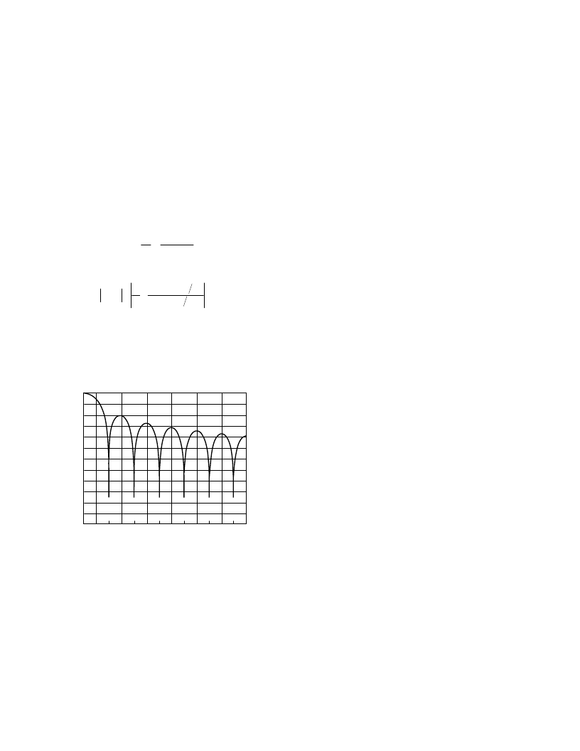
Figure 4 shows the filter frequency response for a cutoff
frequency of 2.62Hz which corresponds to a first filter notch
frequency of 10Hz. The plot is shown from dc to 65Hz.
This response is repeated at either side of the input sampling
frequency and at either side of multiples of the input sampling
frequency.
FREQUENCY – Hz
0
60
0
–40
50
30
20
10
40
–60
–80
–100
–120
–140
–160
–180
–200
–220
–240
–20
G
Figure 4. Frequency Response of AD7714 Filter
The response of the filter is similar to that of an averaging filter
but with a sharper roll-off. The output rate for the digital filter
corresponds with the positioning of the first notch of the filter’s
frequency response. Thus, for the plot of Figure 4 where the
output rate is 10Hz, the first notch of the filter is at 10Hz. The
notches of this (sinx/x)
3
filter are repeated at multiples of the
first notch. The filter provides attenuation of better than 100 dB
at these notches. For the example given, if the first notch is at
10Hz, there will be notches (and hence >100dB rejection) at
both 50Hz and 60Hz.
相關(guān)PDF資料 |
PDF描述 |
|---|---|
| AD7715ARU-3 | 3 V/5 V, 450 uA 16-Bit, Sigma-Delta ADC |
| AD7715ARU-5 | AB 4C 4#12 PIN RECP |
| AD7715AN-3 | 3 V/5 V, 450 uA 16-Bit, Sigma-Delta ADC |
| AD7715AN-5 | 3 V/5 V, 450 uA 16-Bit, Sigma-Delta ADC |
| AD7715AR-3 | 3 V/5 V, 450 uA 16-Bit, Sigma-Delta ADC |
相關(guān)代理商/技術(shù)參數(shù) |
參數(shù)描述 |
|---|---|
| AD7714ACHIPS-3 | 制造商:AD 制造商全稱:Analog Devices 功能描述:3 V/5 V, CMOS, 500 uA Signal Conditioning ADC |
| AD7714ACHIPS-5 | 制造商:AD 制造商全稱:Analog Devices 功能描述:3 V/5 V, CMOS, 500 uA Signal Conditioning ADC |
| AD7714AN-3 | 制造商:Rochester Electronics LLC 功能描述:24-BIT SIGMA DELTA A/D IC - Bulk 制造商:Analog Devices 功能描述: |
| AD7714AN5 | 制造商:ANA 功能描述:24 BIT, 1KSPS, DIP 24 |
發(fā)布緊急采購,3分鐘左右您將得到回復(fù)。