- 您現(xiàn)在的位置:買賣IC網(wǎng) > PDF目錄375235 > AD629BRZ-RL (ANALOG DEVICES INC) High Common-Mode Voltage, Difference Amplifier PDF資料下載
參數(shù)資料
| 型號: | AD629BRZ-RL |
| 廠商: | ANALOG DEVICES INC |
| 元件分類: | 運動控制電子 |
| 英文描述: | High Common-Mode Voltage, Difference Amplifier |
| 中文描述: | OP-AMP, 1000 uV OFFSET-MAX, PDSO8 |
| 封裝: | ROHS COMPLIANT, PLASTIC, MS-012AA, SOIC-8 |
| 文件頁數(shù): | 12/16頁 |
| 文件大?。?/td> | 415K |
| 代理商: | AD629BRZ-RL |
AD629
OUTPUT CURRENT AND BUFFERING
The AD629 is designed to drive loads of 2 kΩ to within 2 V of
the rails but can deliver higher output currents at lower output
voltages (see Figure 15). If higher output current is required, the
output of the AD629 should be buffered with a precision op amp,
such as the OP113, as shown in Figure 36. This op amp can swing
to within 1 V of either rail while driving a load as small as 600 Ω.
Rev. B | Page 12 of 16
REF (–)
REF (+)
–V
S
–V
S
+V
S
V
OUT
NC
–IN
+IN
0.1μF
0.1μF
0.1μF
0.1μF
NC = NO CONNECT
21.1k
380k
380k
20k
380k
AD629
1
2
3
4
8
7
6
5
0
OP113
Figure 36. Output Buffering Application
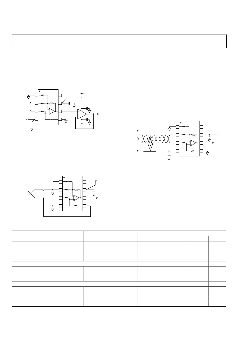
A GAIN OF 19 DIFFERENTIAL AMPLIFIER
While low level signals can be connected directly to the –IN and
+IN inputs of the AD629, differential input signals can also be
connected, as shown in Figure 37, to give a precise gain of 19.
However, large common-mode voltages are no longer permissible.
Cold junction compensation can be implemented using a
temperature sensor, such as the
AD590
.
REF (–)
REF (+)
+V
S
+V
S
NC
–IN
+IN
0.1μF
NC = NO CONNECT
21.1k
380k
380k
20k
380k
AD629
1
2
3
4
8
7
6
5
0
V
OUT
V
REF
THERMOCOUPLE
Figure 37. A Gain of 19 Thermocouple Amplifier
ERROR BUDGET ANALYSIS EXAMPLE 1
In the dc application that follows, the 10 A output current from
a device with a high common-mode voltage (such as a power
supply or current-mode amplifier) is sensed across a 1 Ω shunt
resistor (see Figure 38). The common-mode voltage is 200 V,
and the resistor terminals are connected through a long pair of
lead wires located in a high noise environment, for example,
50 Hz/60 Hz, 440 V ac power lines. The calculations in Table 5
assume an induced noise level of 1 V at 60 Hz on the leads, in
addition to a full-scale dc differential voltage of 10 V. The error
budget table quantifies the contribution of each error source.
Note that the dominant error source in this example is due to
the dc common-mode voltage.
REF (–)
OUTPUT
CURRENT
60Hz
POWER LINE
1
SHUNT
REF (+)
–V
S
+V
S
V
OUT
NC
–IN
+IN
0.1μF
0.1μF
NC = NO CONNECT
21.1k
380k
380k
20k
380k
AD629
1
2
3
4
8
7
6
5
0
10 AMPS
200V
DC
TO GROUND
Figure 38. Error Budget Analysis Example 1: V
IN
= 10 V Full-Scale,
V
CM
= 200 V DC, R
SHUNT
= 1 Ω, 1 V p-p, 60 Hz Power-Line Interference
Table 5. AD629 vs. INA117 Error Budget Analysis Example 1 (V
CM
= 200 V dc)
Error Source
ACCURACY, T
A
= 25°C
Initial Gain Error
Offset Voltage
DC CMR (Over Temperature)
TEMPERATURE DRIFT (85°C)
Gain
Offset Voltage
RESOLUTION
Noise, Typical, 0.01 Hz to 10 Hz, μV p-p
CMR, 60 Hz
Nonlinearity
AD629
(0.0005 × 10)/10 V × 10
6
(0.001 V/10 V) × 10
6
(224 × 10
-6
× 200 V)/10 V × 10
6
10 ppm/°C × 60°C
(20 μV/°C × 60°C) × 10
6
/10 V
15 μV/10 V × 10
6
(141 × 10
-6
× 1 V)/10 V × 10
6
(10
-5
× 10 V)/10 V × 10
6
INA117
(0.0005 × 10)/10 V × 10
6
(0.002 V/10 V) × 10
6
(500 × 10
-6
× 200 V)/10 V × 10
6
Total Accuracy Error
10 ppm/°C × 60°C
(40 μV/°C × 60°C) × 10
6
/10 V
Total Drift Error
25 μV/10 V × 10
6
(500 × 10
-6
× 1 V)/10 V × 10
6
(10
-5
× 10 V)/10 V × 10
6
Total Resolution Error
Total Error
Error, ppm of FS
AD629
500
100
4480
5080
600
120
720
2
14
10
26
5826
INA117
500
200
10,000
10,700
600
240
840
3
50
10
63
11,603
相關(guān)PDF資料 |
PDF描述 |
|---|---|
| AD629-EVAL | High Common-Mode Voltage, Difference Amplifier |
| AD6315QF | 1/4- to 1/12 Duty VFD Controller/Driver |
| AD6315 | 1/4- to 1/12 Duty VFD Controller/Driver |
| AD6315L | 1/4- to 1/12 Duty VFD Controller/Driver |
| AD6315LF | 1/4- to 1/12 Duty VFD Controller/Driver |
相關(guān)代理商/技術(shù)參數(shù) |
參數(shù)描述 |
|---|---|
| AD629-EVAL | 制造商:Analog Devices 功能描述: |
| AD62BS | 制造商:POP 功能描述: |
| AD62H | 制造商:POP 功能描述: |
| AD63 | 制造商:MQP (ELECTRONICS) 功能描述:ADAPTOR DIL 32WAY 制造商:MQP (ELECTRONICS) 功能描述:ADAPTOR, DIL, 32WAY 制造商:MQP (ELECTRONICS) 功能描述:ADAPTOR, DIL, 32WAY; Connector Type:Adaptor; No. of Contacts:32; Row Pitch:0.6"; Contact Termination:Through Hole Vertical; SVHC:No SVHC (19-Dec-2012); Connector Mounting Orientation:PC Board; No. of Ways:32; Package / Case:DIL; Pin ;RoHS Compliant: Yes |
| AD63 | 制造商:MQP (ELECTRONICS) 功能描述:ADAPTOR DIL 32 WAY |
發(fā)布緊急采購,3分鐘左右您將得到回復(fù)。