- 您現(xiàn)在的位置:買賣IC網(wǎng) > PDF目錄362053 > AC162834ADGG (NXP SEMICONDUCTORS) 18-bit registered driver with inverted register enable and 30ohm termination resistors 3-State PDF資料下載
參數(shù)資料
| 型號: | AC162834ADGG |
| 廠商: | NXP SEMICONDUCTORS |
| 元件分類: | 通用總線功能 |
| 英文描述: | 18-bit registered driver with inverted register enable and 30ohm termination resistors 3-State |
| 中文描述: | ALVC/VCX/A SERIES, 18-BIT DRIVER, TRUE OUTPUT, PDSO56 |
| 封裝: | 6.10 MM, PLASTIC, SOT-364-1, TSSOP2-56 |
| 文件頁數(shù): | 8/12頁 |
| 文件大小: | 122K |
| 代理商: | AC162834ADGG |
Philips Semiconductors
Product specification
74ALVC162834A
18-bit registered driver with inverted register enable
and 30
termination resistors (3-State)
2000 Mar 14
8
AC WAVEFORMS FOR V
CC
= 3.0 V TO 3.6 V AND
V
CC
= 2.7 V
V
M
= 1.5 V
V
X
= V
OL
+ 0.3 V
V
Y
= V
OH
– 0.3 V
V
OL
and V
OH
are the typical output voltage drop that occur with the
output load.
V
I
= 2.7 V
AC WAVEFORMS FOR V
CC
= 2.3 V TO 2.7 V AND
V
CC
< 2.3 V RANGE
V
M
= 0.5 V
CC
V
X
= V
OL
+ 0.15 V
V
Y
= V
– 0.15 V
V
and V
OH
are the typical output voltage drop that occur with the
output load.
V
I
= V
CC
A
INPUT
t
PHL
t
PLH
V
OL
V
I
GND
V
OH
Y
OUTPUT
SH00132
V
M
V
M
NOTE: V
M
= 0.5V
CC
at V
CC
= 2.3 to 2.7 V
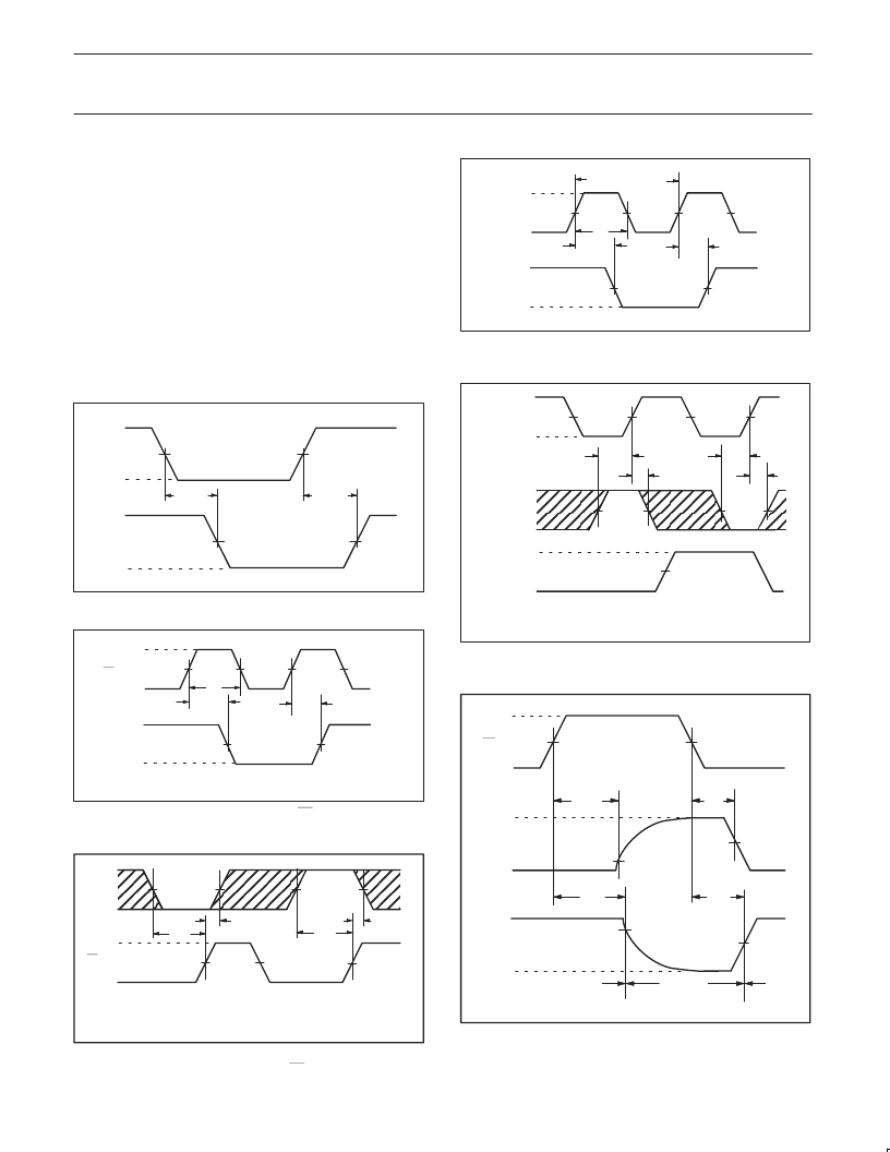
Waveform 1. Input (An) to output (Yn) propagation delay
LE INPUT
Yn OUTPUT
V
I
GND
V
OH
V
OL
t
PHL
t
PLH
t
W
V
M
V
M
V
M
SH00165
NOTE: V
M
= 0.5 V
CC
at V
CC
= 2.3 to 2.7 V
Waveform 2. Latch enable input (LE) pulse width,
the latch enable input to output (Yn) propagation delays.
ééé
ééé
ééé
GND
éééééééé
éééééééé
éééééééé
An
INPUT
LE
INPUT
t
SU
NOTE:
The shaded areas indicate when the input is permitted to change
for predictable output performance.
V
M
= 0.5V
CC
at V
CC
= 2.3 to 2.7 V
t
SU
V
V
I
GND
V
V
M
SH00166
Waveform 3. Data set-up and hold times
for the An input to the LE input
CP INPUT
Yn OUTPUT
V
I
GND
V
OH
V
OL
t
PHL
t
PLH
t
W
1/f
MAX
SH00135
V
M
V
M
V
M
NOTE: V
M
= 0.5V
CC
at V
CC
= 2.3 to 2.7 V
Waveform 4. The clock (CP) to Yn propagation delays,
the clock pulse width and the maximum clock frequency.
V
I
GND
éééé
éééé
éééé
ééééééé
ééééééé
ééééééé
An INPUT
V
I
GND
V
OH
Yn OUTPUT
V
OL
CP INPUT
t
su
t
h
t
su
t
h
NOTE:
The shaded areas indicate when the input is permitted to change
for predictable output performance.
V
M
= 0.5V
CC
at V
CC
= 2.3 to 2.7 V
SH00136
V
M
V
M
Waveform 5. Data set-up and hold times for the An input to the
clock CP input
t
PLZ
t
PZL
V
I
nOE INPUT
GND
V
CC
OUTPUT
LOW-to-OFF
OFF-to-LOW
V
OL
V
OH
OUTPUT
HIGH-to-OFF
OFF-to-HIGH
GND
outputs
enabled
outputs
enabled
outputs
disabled
t
PHZ
V
M
V
M
V
M
t
PZH
V
X
V
Y
SH00137
NOTE: V
M
= 0.5V
CC
at V
CC
= 2.3 to 2.7 V
Waveform 6. 3-State enable and disable times
相關(guān)PDF資料 |
PDF描述 |
|---|---|
| AC164010 | SOCKELMODUL |
| AC164012 | SOCKELMODUL |
| AC164026 | SOCKET MODULE SOIC/TSSOP |
| AC174002 | SOCKELMODUL |
| AC164001 | SOCKELMODUL |
相關(guān)代理商/技術(shù)參數(shù) |
參數(shù)描述 |
|---|---|
| AC-162A | 制造商:ZETTLER 制造商全稱:ZETTLER Electronics 功能描述:SPECIFICATIONS FOR LCD MODULE |
| AC-162B | 制造商:ZETTLER 制造商全稱:ZETTLER Electronics 功能描述:SPECIFICATIONS FOR LCD MODULE |
| AC-162C | 制造商:ZETTLER 制造商全稱:ZETTLER Electronics 功能描述:SPECIFICATIONS FOR LCD MODULE |
| AC-162D | 制造商:ZETTLER 制造商全稱:ZETTLER Electronics 功能描述:SPECIFICATIONS FOR LCD MODULE |
| AC-162DGA | 制造商:ZETTLER 制造商全稱:ZETTLER Electronics 功能描述:SPECIFICATIONS FOR LCD MODULE |
發(fā)布緊急采購,3分鐘左右您將得到回復(fù)。