- 您現(xiàn)在的位置:買賣IC網(wǎng) > PDF目錄375225 > AC12BGML Thyristor Product Catalog PDF資料下載
參數(shù)資料
| 型號: | AC12BGML |
| 英文描述: | Thyristor Product Catalog |
| 中文描述: | 晶閘管產品目錄 |
| 文件頁數(shù): | 121/224頁 |
| 文件大?。?/td> | 2697K |
| 代理商: | AC12BGML |
第1頁第2頁第3頁第4頁第5頁第6頁第7頁第8頁第9頁第10頁第11頁第12頁第13頁第14頁第15頁第16頁第17頁第18頁第19頁第20頁第21頁第22頁第23頁第24頁第25頁第26頁第27頁第28頁第29頁第30頁第31頁第32頁第33頁第34頁第35頁第36頁第37頁第38頁第39頁第40頁第41頁第42頁第43頁第44頁第45頁第46頁第47頁第48頁第49頁第50頁第51頁第52頁第53頁第54頁第55頁第56頁第57頁第58頁第59頁第60頁第61頁第62頁第63頁第64頁第65頁第66頁第67頁第68頁第69頁第70頁第71頁第72頁第73頁第74頁第75頁第76頁第77頁第78頁第79頁第80頁第81頁第82頁第83頁第84頁第85頁第86頁第87頁第88頁第89頁第90頁第91頁第92頁第93頁第94頁第95頁第96頁第97頁第98頁第99頁第100頁第101頁第102頁第103頁第104頁第105頁第106頁第107頁第108頁第109頁第110頁第111頁第112頁第113頁第114頁第115頁第116頁第117頁第118頁第119頁第120頁當前第121頁第122頁第123頁第124頁第125頁第126頁第127頁第128頁第129頁第130頁第131頁第132頁第133頁第134頁第135頁第136頁第137頁第138頁第139頁第140頁第141頁第142頁第143頁第144頁第145頁第146頁第147頁第148頁第149頁第150頁第151頁第152頁第153頁第154頁第155頁第156頁第157頁第158頁第159頁第160頁第161頁第162頁第163頁第164頁第165頁第166頁第167頁第168頁第169頁第170頁第171頁第172頁第173頁第174頁第175頁第176頁第177頁第178頁第179頁第180頁第181頁第182頁第183頁第184頁第185頁第186頁第187頁第188頁第189頁第190頁第191頁第192頁第193頁第194頁第195頁第196頁第197頁第198頁第199頁第200頁第201頁第202頁第203頁第204頁第205頁第206頁第207頁第208頁第209頁第210頁第211頁第212頁第213頁第214頁第215頁第216頁第217頁第218頁第219頁第220頁第221頁第222頁第223頁第224頁
2002 Teccor Electronics
Thyristor Product Catalog
AN1001 - 1
http://www.teccor.com
+1 972-580-7777
AN1001
Fundamental Characteristics of Thyristors
Introduction
The thyristor family of semiconductors consists of several very
useful devices. The most widely used of this family are silicon
controlled rectifiers (SCRs), triacs, sidacs, and diacs. In many
applications these devices perform key functions and are real
assets in meeting environmental, speed, and reliability specifica-
tions which their electro-mechanical counterparts cannot fulfill.
This application note presents the basic fundamentals of SCR,
triac, sidac, and diac thyristors so the user understands how they
differ in characteristics and parameters from their electro-
mechanical counterparts. Also, thyristor terminology is defined.
SCR
Basic Operation
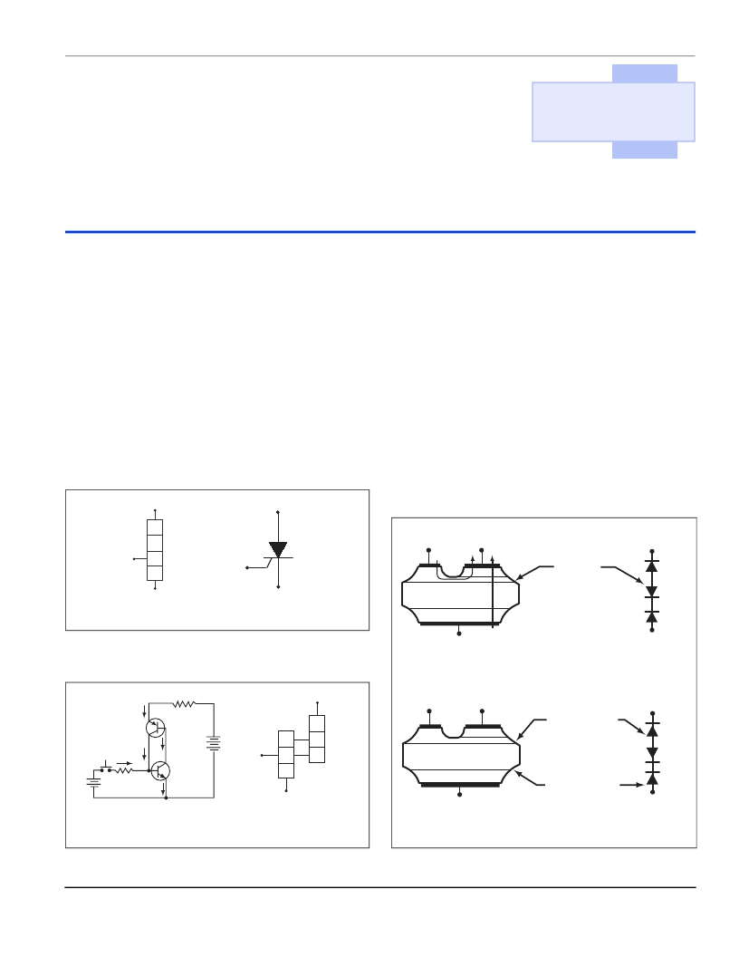
Figure AN1001.1 shows the simple block construction of an SCR.
Figure AN1001.1
SCR Block Construction
The operation of a PNPN device can best be visualized as a spe-
cially coupled pair of transistors as shown in Figure AN1001.2.
Figure AN1001.2
Coupled Pair of Transistors as a SCR
The connections between the two transistors trigger the occur-
rence of regenerative action when a proper gate signal is applied
to the base of the NPN transistor. Normal leakage current is so
low that the combined h
of the specially coupled two-transistor
feedback amplifier is less than unity, thus keeping the circuit in
an off-state condition. A momentary positive pulse applied to the
gate biases the NPN transistor into conduction which, in turn,
biases the PNP transistor into conduction. The effective h
FE
momentarily becomes greater than unity so that the specially
coupled transistors saturate. Once saturated, current through the
transistors is enough to keep the combined h
FE
greater than
unity. The circuit remains “on” until it is “turned off” by reducing
the anode-to-cathode current (I
) so that the combined h
is less
than unity and regeneration ceases. This threshold anode current
is the holding current of the SCR.
Geometric Construction
Figure AN1001.3 shows cross-sectional views of an SCR chip
and illustrations of current flow and junction biasing in both the
blocking and triggering modes.
Figure AN1001.3
Cross-sectional View of SCR Chip
Gate
Gate
J1
J2
J3
P
N
P
N
Schematic Symbol
Block Construction
Cathode
Anode
Cathode
Anode
N
P
N
P
N
P
Gate
Cathode
J1
J2
J2
J3
Anode
N
N
N
Cathode
Gate
Anode
Load
P
P
Two-transistor
Schematic
Two-transistor Block
Construction Equivalent
Gate
(+)
Cathode
(-)
IGT
P
N
N
P
(+)
(+)
Anode
IT
Forward Bias and Current Flow
Gate
Cathode
P
N
N
P
(-)
Anode
Reverse Bias
Reverse Biased
Junction
(-)
Anode
Equivalent Diode
Relationship
Forward
Blocking
Junction
Cathode
(-)
(+)
Anode
Equivalent Diode
Relationship
Cathode
(+)
Reverse Biased
Gate Junction
AN1001
相關PDF資料 |
PDF描述 |
|---|---|
| AC12BSM | Thyristor Product Catalog |
| AC12DGML | Thyristor Product Catalog |
| AC12DSM | MAX CLIP RoHS Compliant: Yes NC/NR |
| AC12EGML | Thyristor Product Catalog |
| AC12ESM | Thyristor Product Catalog |
相關代理商/技術參數(shù) |
參數(shù)描述 |
|---|---|
| AC12BSM | 制造商:TECCOR 制造商全稱:TECCOR 功能描述:Thyristor Product Catalog |
| AC12DGM | 制造商:NEC 制造商全稱:NEC 功能描述:12A MOLD TRIAC |
| AC12DGML | 制造商:TECCOR 制造商全稱:TECCOR 功能描述:Thyristor Product Catalog |
| AC12DSM | 制造商:TECCOR 制造商全稱:TECCOR 功能描述:Thyristor Product Catalog |
| AC12DSMA | 制造商:NEC 制造商全稱:NEC 功能描述:12A RESIN INSULATION TYPE TRIAC |
發(fā)布緊急采購,3分鐘左右您將得到回復。