- 您現(xiàn)在的位置:買(mǎi)賣IC網(wǎng) > PDF目錄375142 > A49LF004TX-33C (AMIC Technology Corporation) 4 Mbit CMOS 3.3Volt-only Firmware Hub Flash Memory PDF資料下載
參數(shù)資料
| 型號(hào): | A49LF004TX-33C |
| 廠商: | AMIC Technology Corporation |
| 英文描述: | 4 Mbit CMOS 3.3Volt-only Firmware Hub Flash Memory |
| 中文描述: | 4兆位的CMOS 3.3Volt只閃存固件集線器 |
| 文件頁(yè)數(shù): | 12/32頁(yè) |
| 文件大?。?/td> | 595K |
| 代理商: | A49LF004TX-33C |
第1頁(yè)第2頁(yè)第3頁(yè)第4頁(yè)第5頁(yè)第6頁(yè)第7頁(yè)第8頁(yè)第9頁(yè)第10頁(yè)第11頁(yè)當(dāng)前第12頁(yè)第13頁(yè)第14頁(yè)第15頁(yè)第16頁(yè)第17頁(yè)第18頁(yè)第19頁(yè)第20頁(yè)第21頁(yè)第22頁(yè)第23頁(yè)第24頁(yè)第25頁(yè)第26頁(yè)第27頁(yè)第28頁(yè)第29頁(yè)第30頁(yè)第31頁(yè)第32頁(yè)
A49LF004
PRELIMINARY (November, 2003, Version 0.0)
11
AMIC Technology, Corp.
Table 7: A/A Mux Mode Operation Selection
Block-Erase Operation
The Block-Erase Operation allows the system to erase the
device in 64 KByte uniform block size for the A49LF004. The
Block-Erase operation is initiated by executing a six-byte
command load sequence for Software Data Protection with
Block-Erase command (30H or 50H) and block address. The
internal Block-Erase operation begins after the sixth WE# pulse.
The End-of-Erase can be determined using either Data# Polling
or Toggle Bit methods. See Figure 15 for timing waveforms.
Any commands written during the Block- Erase operation will
be ignored.
Chip-Erase
The A49LF004 device provides a Chip-Erase operation only in
A/A Mux mode, which allows the user to erase the entire
memory array to the ‘1’s state. This is useful when the entire
device must be quickly erased. The Chip-Erase operation is
initiated by executing a six-byte Software Data Protection
command sequence with Chip-Erase command (10H) with
address 5555H in the last byte sequence. The internal Erase
operation begins with the rising edge of the sixth WE#. During
the internal Erase operation, the only valid read is Toggle Bit or
Data# Polling. See Table 8 for the command sequence, Figure
16 for timing diagram, and Figure 21 for the flowchart. Any
commands written during the Chip-Erase operation will be
ignored.
Write Operation Status Detection
The A49LF004 device provides two software means to detect
the completion of a Write (Program or Erase) cycle, in
order to optimize the system Write cycle time. The software
detection includes two status bits: Data# Polling (I/O
7
) and
Toggle Bit (I/O
6
). The End-of-Write detection mode is enabled
after the rising edge of WE# which initiates the internal Program
or Erase operation. The actual completion of the nonvolatile
write is asynchronous with the system; therefore, either a Data#
Polling or Toggle Bit read may be simultaneous with the
completion of the Write cycle. If this occurs, the system may
possibly get an erroneous result, i.e., valid data may appear to
conflict with either I/O
7
or I/O
6
. In order to prevent spurious
rejection, if an erroneous result occurs, the software routine
should include a loop to read the accessed location an
additional two times. If both reads are valid, then the device has
completed the Write cycle, otherwise the rejection is valid.
Data# Polling (I/O
7
)
When the A49LF004 device is in the internal Program operation,
any attempt to read I/O
7
will produce the complement of the
true data. Once the Program operation is completed, I/O
7
will
produce true data. Note that even though I/O
7
may have valid
data immediately following the completion of an internal Write
operation, the remaining data outputs may still be invalid: valid
data on the entire data bus will appear in subsequent
successive Read cycles after an interval of 1 μs. During internal
Erase operation, any attempt to read I/O
7
will produce a ‘0’.
Once the internal Erase operation is completed, I/O
7
will
produce a ‘1’. The Data# Polling is valid after the rising edge of
fourth WE# pulse for Program operation. For Block- or Chip-
Erase, the Data# Polling is valid after the rising edge of sixth
WE# pulse. See Figure 12 for Data# Polling timing diagram.
Proper status will not be given using Data# Polling if the
address is in the invalid range.
Toggle Bit (I/O
6
)
During the internal Program or Erase operation, any
consecutive attempts to read I/O
6
will produce alternating ‘0’s
and ‘1’s, i.e., toggling between 0 and 1. When the internal
Program or Erase operation is completed, the toggling will stop.
The device is then ready for the next operation. The Toggle Bit
is valid after the rising edge of fourth WE# pulse for Program
operation. For Block- or Chip-Erase, the Toggle Bit is valid after
the rising edge of sixth WE# pulse. See Figure 13 for Toggle Bit
timing diagram.
Data Protection
The A49LF004 device provides both hardware and software
features to protect nonvolatile data from inadvertent writes.
Hardware Data Protection
Noise/Glitch Protection: A WE# pulse of less than 5 ns will not
initiate a Write cycle.
V
DD
Power Up/Down Detection: The Write operation is inhibited
when V
DD
is less than 1.5V.
Write Inhibit Mode: Forcing OE# low, WE# high will inhibit the
Write operation. This prevents inadvertent writes during power-
up or power-down.
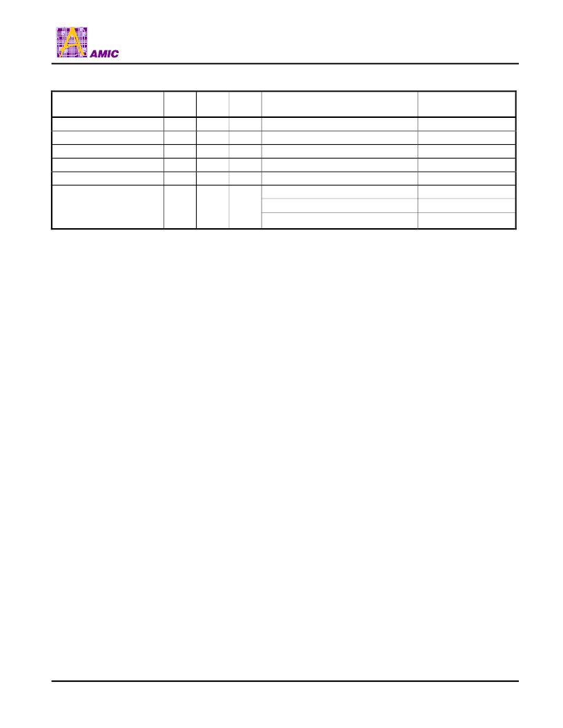
Mode
RST#
OE#
WE#
Address
I/O
Read
V
IH
V
IH
V
IH
V
IH
V
IL
V
IL
V
IH
V
IH
V
IH
X
V
IH
V
IL
V
IH
X
A
IN
A
IN
X
D
OUT
D
IN
High Z
Write
Standby
Output Disable
X
High Z
Reset
X
X
High Z
A21 – A2 = X, A1 = V
IL
, A0 = V
IL
Manufacturer ID
A21 – A2 = X, A1 = V
IL
, A0 = V
IH
Device ID
Product Identification
V
IH
V
IL
V
IH
A21 – A2 = X, A1 = V
IH
, A0 = V
IH
Continuation ID
相關(guān)PDF資料 |
PDF描述 |
|---|---|
| A49LF004TL-33C | 4 Mbit CMOS 3.3Volt-only Firmware Hub Flash Memory |
| A49LF004 | 4 Mbit CMOS 3.3Volt-only Firmware Hub Flash Memory |
| A49LF040A | 4 Mbit CMOS 3.3Volt-only Low Pin Count Flash Memory |
| A49LF040ATL-33 | 4 Mbit CMOS 3.3Volt-only Low Pin Count Flash Memory |
| A49LF040ATL-33F | 4 Mbit CMOS 3.3Volt-only Low Pin Count Flash Memory |
相關(guān)代理商/技術(shù)參數(shù) |
參數(shù)描述 |
|---|---|
| A49LF040 | 制造商:AMICC 制造商全稱:AMIC Technology 功能描述:4 Mbit CMOS 3.3Volt-only Low Pin Count Flash Memory |
| A49LF040A | 制造商:AMICC 制造商全稱:AMIC Technology 功能描述:4 Mbit CMOS 3.3Volt-only Low Pin Count Flash Memory |
| A49LF040ATL-33 | 制造商:AMICC 制造商全稱:AMIC Technology 功能描述:4 Mbit CMOS 3.3Volt-only Low Pin Count Flash Memory |
| A49LF040ATL-33F | 制造商:AMICC 制造商全稱:AMIC Technology 功能描述:4 Mbit CMOS 3.3Volt-only Low Pin Count Flash Memory |
| A49LF040ATX-33 | 制造商:AMICC 制造商全稱:AMIC Technology 功能描述:4 Mbit CMOS 3.3Volt-only Low Pin Count Flash Memory |
發(fā)布緊急采購(gòu),3分鐘左右您將得到回復(fù)。